

Thread
5 boards to have a crack at
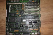
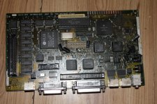
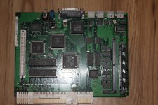
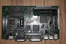
these are not my boards. they belong to rollermanz.
he says that he put the color classic into an oven to dry it after washing and it caught on fire in the oven
looks like it was plugged in to me
-
the pictures show the boards as I got them.
-
im trying to get some of them working again..........but right now I am working on one of the se/30 boards and ive just discovered that some of the chips have been swapped from one boards to the other.
-
rollermanz....................the 2 se/30 boards....................did you swap any chips from one board to another ?
he says that he put the color classic into an oven to dry it after washing and it caught on fire in the oven
looks like it was plugged in to me
-
the pictures show the boards as I got them.
-
im trying to get some of them working again..........but right now I am working on one of the se/30 boards and ive just discovered that some of the chips have been swapped from one boards to the other.
-
rollermanz....................the 2 se/30 boards....................did you swap any chips from one board to another ?
hey techknight - yep.. have to agree
-
theres chips , crystals, transistors missing, chips swapped...........all the boards are totally covered in a thick brown goo. I think he used a plumbers flux at the start but he got better as he went. Looks like the classic 2 was the last board
-
im working on one of the se/30 - just replaced 2 of the chips by the battery - uj2 f258 and uj3 f258. Do you know what they do.....there are 6 of them, all the same
-
theres chips , crystals, transistors missing, chips swapped...........all the boards are totally covered in a thick brown goo. I think he used a plumbers flux at the start but he got better as he went. Looks like the classic 2 was the last board
-
im working on one of the se/30 - just replaced 2 of the chips by the battery - uj2 f258 and uj3 f258. Do you know what they do.....there are 6 of them, all the same
both se/30's are dead.
-
the first due to an acid lead around the battery. All the solder on the pins from the rom connector is rotten, loads of via's. Feck it , you could spend all dam year on it
-
second board looked good....at first. No acid leak.
-
started replacing the chips missing until I got to ue8.
-
ue8 is missing...........along with over 10 of its pads.....not only that but most of the traces from those pads. 2 of the pads are still there, hanging on the end of the trace that is just hanging in space.
-
looks like the ue8 was torn off the board
-
such a pity.
-
will have a go at the classic 2 tomorrow - looks like no acid leak and no missing parts.
-
the first due to an acid lead around the battery. All the solder on the pins from the rom connector is rotten, loads of via's. Feck it , you could spend all dam year on it
-
second board looked good....at first. No acid leak.
-
started replacing the chips missing until I got to ue8.
-
ue8 is missing...........along with over 10 of its pads.....not only that but most of the traces from those pads. 2 of the pads are still there, hanging on the end of the trace that is just hanging in space.
-
looks like the ue8 was torn off the board
-
such a pity.
-
will have a go at the classic 2 tomorrow - looks like no acid leak and no missing parts.

that's just what I found techknight - all the pins from the rom holder are all blackened and the solder is a dark grey...rotton.On 3 pins it was almost completely gone. I resoldered those. All the via's around the battery are all dark grey and 'flakey'
is there any way to renew the solder in a via and make it good again?
Ive tried pressing soldering tip into each via, small amount of force, and turn clockwise and anti clockwise. Sometimes it forces shiny solder to the surface.....sometimes it does not. Don't know if it is making things worse.
I imagine the only fix is to meter every connection and then bridge any broken ones.........that would take allot of time and still might not work.
is solder in this condition destroyed , as in non conductive. Fresh new solder will not melt into it, even with flux. It does not want to stick to copper or anything.
Is there any other alternative. There must be a way to remove this bad solder and replace it with new solder
-
thoes dam batteries have allot to answer for!!
is there any way to renew the solder in a via and make it good again?
Ive tried pressing soldering tip into each via, small amount of force, and turn clockwise and anti clockwise. Sometimes it forces shiny solder to the surface.....sometimes it does not. Don't know if it is making things worse.
I imagine the only fix is to meter every connection and then bridge any broken ones.........that would take allot of time and still might not work.
is solder in this condition destroyed , as in non conductive. Fresh new solder will not melt into it, even with flux. It does not want to stick to copper or anything.
Is there any other alternative. There must be a way to remove this bad solder and replace it with new solder
-
thoes dam batteries have allot to answer for!!
You cant really fix the via. the SE/30 uses a multi-layer board, and the traces back to the CPU is run in the middle layer. you cant see them.
So, Sometimes you can stick a small thin piece of wire through the via, and tack it to the traces on both sides, snipping the wire off at the joint. IF... and only IF... that via still has a good connection back to the cpu.
If not, then you stick a piece of wire through as I explained above, soldering it to both sides of traces, but leave the wire in tact and run it back to the CPU.
So, Sometimes you can stick a small thin piece of wire through the via, and tack it to the traces on both sides, snipping the wire off at the joint. IF... and only IF... that via still has a good connection back to the cpu.
If not, then you stick a piece of wire through as I explained above, soldering it to both sides of traces, but leave the wire in tact and run it back to the CPU.
theres 3 layers.................darn.....did not know that. thought it was just 2
-
and each via is a connection point between all 3 layers?...........that just makes them more prone to any kind of acid leak damage..............no wonder the se30 board has wrecked my head way more than any other mac
-
come to think of it..............it makes sense now. I was looking at some via's (the 7 just next to the rom slot) on one side of the board they have no traces leading away from them. on the other only 3 have traces heading to the rom slot. I thought the other 4 were not used as I saw no traces on either side of the board. From what you just explained it makes more sense now.
-
makes more sense.............but my head hurts more now.
-
I got a different se30 working last year by melting pins into vias. It was on the ue8. I used the wire from new caps. hold it on the via, heat it , and it slowly sank into the via. snipped off the wire to the right length and bent it to reach the pin of the ue8. soldered it directly onto the pin. Think I had to do 5 to restore the display.
-
out of curiosity is there a diagram of the hidden layer anywhere.
-
cheers techknight
-
and each via is a connection point between all 3 layers?...........that just makes them more prone to any kind of acid leak damage..............no wonder the se30 board has wrecked my head way more than any other mac
-
come to think of it..............it makes sense now. I was looking at some via's (the 7 just next to the rom slot) on one side of the board they have no traces leading away from them. on the other only 3 have traces heading to the rom slot. I thought the other 4 were not used as I saw no traces on either side of the board. From what you just explained it makes more sense now.
-
makes more sense.............but my head hurts more now.
-
I got a different se30 working last year by melting pins into vias. It was on the ue8. I used the wire from new caps. hold it on the via, heat it , and it slowly sank into the via. snipped off the wire to the right length and bent it to reach the pin of the ue8. soldered it directly onto the pin. Think I had to do 5 to restore the display.
-
out of curiosity is there a diagram of the hidden layer anywhere.
-
cheers techknight
No, its 4 layers. But the inner two layers share VCC/Ground/Traces.
Yes, the vias are connecting all 4 layers. BUT, there is an annular ring gap on the layers that dont intersect the via.
Try working on modern boards. They are 6+ layers, and have hidden vias. Vias between layers that dont protrude to the top and bottom.
As far as diagram, Nope. you will have to follow the schematic.
BTW, all mac logic boards are at least 4 layers.
The reason they decided to run traces inner layer, is so they didnt have to weave the traces top-bottom-top-bottom alongside the traces that already are on the top and bottom. This is basically to prevent race conditions that occur when you do that alot.
On modern super speed systems, notice the traces between processors/RAM/ROM are meandered. look like squiggly S. This is keep all the trace "lengths" identical between all pin connections to one another. For this very reason.
on modern high speed systems, thats a requirement. You would need an advanced cad package like Altium or something of the like, and the autorouter do to that for you
if you do it manually, well, good luck. lol.
Trust me, ive ran down battery damaged SE/30 boards and got them running again, I feel your pain.
Yes, the vias are connecting all 4 layers. BUT, there is an annular ring gap on the layers that dont intersect the via.
Try working on modern boards. They are 6+ layers, and have hidden vias. Vias between layers that dont protrude to the top and bottom.
As far as diagram, Nope. you will have to follow the schematic.
BTW, all mac logic boards are at least 4 layers.
The reason they decided to run traces inner layer, is so they didnt have to weave the traces top-bottom-top-bottom alongside the traces that already are on the top and bottom. This is basically to prevent race conditions that occur when you do that alot.
On modern super speed systems, notice the traces between processors/RAM/ROM are meandered. look like squiggly S. This is keep all the trace "lengths" identical between all pin connections to one another. For this very reason.
on modern high speed systems, thats a requirement. You would need an advanced cad package like Altium or something of the like, and the autorouter do to that for you
if you do it manually, well, good luck. lol.
Trust me, ive ran down battery damaged SE/30 boards and got them running again, I feel your pain.
your a wealth of info man. 6 layers!!!! .........ill stick with macs. Got my hands on an IBM AS/400 the otherday....had a look at the main board......I think its just 2 layers...........but man its just a monster. 10 inch floppy drive (I think)
-
anyway good news..........just got a chime from the second se30........a good chime.........but video=1 line across middle of screen. This is the board with the ue8 ripped off.
replaced it with one from one of my dead se30's along with 2 crystals, uj3 (that was on first se30!!), 2 transistors and a few caps.
-
have a good se30 alongside this one and im metering away at random - good board , pin 1 to anywhere I can find a beep.... then do same continuioty test on bad ue8
-
its 3:36am here in Ireland and im not going to bed until this dam thing works
-
anyway good news..........just got a chime from the second se30........a good chime.........but video=1 line across middle of screen. This is the board with the ue8 ripped off.
replaced it with one from one of my dead se30's along with 2 crystals, uj3 (that was on first se30!!), 2 transistors and a few caps.
-
have a good se30 alongside this one and im metering away at random - good board , pin 1 to anywhere I can find a beep.... then do same continuioty test on bad ue8
-
its 3:36am here in Ireland and im not going to bed until this dam thing works
id say its safe to say its ue8..............10 of its pads are gone............along with their traces
-
have most of them reconnected
-
now I have a broken white line................
-
I have 4 pins left to connect
-
luckily allot of the pads had via's close by. Melt in a bit of wire (cap leg), bend it to the pin of the chip and solder
-
its ugly but its worked before................but never this bad
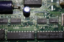
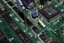
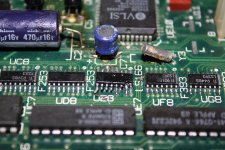
-
have most of them reconnected
-
now I have a broken white line................
-
I have 4 pins left to connect
-
luckily allot of the pads had via's close by. Melt in a bit of wire (cap leg), bend it to the pin of the chip and solder
-
its ugly but its worked before................but never this bad
For what it's worth I recapped an SE/30 recently with a horizontal line on screen-- no change after recap. The culprit turned out to be a via near UF8.
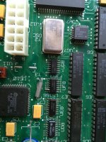
From the schematic, UF8 appears to count vertical lines. The output goes to PAL UG6 which probably implements comparators at 342 and 370 lines to generate the VSYNC pulse. Bad connection from UF8 = no match on the comparator = no VSYNC pulse, I think.
Half-baked idea based on the above: UG7 looks to do something similar for HSYNC. Change the comparators on these two (by lifting VSYNC and HSYNC off the PALs or swapping data lines around) to get larger horizontal and vertical resolution. Then overclock to get back to 22.25kHz horizontal scan rate, though either lower vertical refresh or non-square pixels.
Probably the video memory would be the downfall of that plan though-- not sure it would be big enough. And beyond that, there would be ROM changes to teach the new resolution....
From the schematic, UF8 appears to count vertical lines. The output goes to PAL UG6 which probably implements comparators at 342 and 370 lines to generate the VSYNC pulse. Bad connection from UF8 = no match on the comparator = no VSYNC pulse, I think.
Half-baked idea based on the above: UG7 looks to do something similar for HSYNC. Change the comparators on these two (by lifting VSYNC and HSYNC off the PALs or swapping data lines around) to get larger horizontal and vertical resolution. Then overclock to get back to 22.25kHz horizontal scan rate, though either lower vertical refresh or non-square pixels.
Probably the video memory would be the downfall of that plan though-- not sure it would be big enough. And beyond that, there would be ROM changes to teach the new resolution....
thanks apm...........tested all vias to pins for continuity - they all check out.
-
this board seems not to have any acid leak, and very little electrolyte damage.
-
the main problem is/was.......(and prob always will be) ue8
-
decided to start from scratch today. So removed all caps, ue8 and the pins from the cap legs I used last night
-
cleaned board
-
used very small wires to melt into via's around ue8 and then to solder onto ue8 legs/pins.
-
many pads and traces gone so hade to use wire
-
my problem (among others) is I just used basic continuity test on each pin on a good board to find any point where that pin would connect.
applied this to bad board
and soldered in the wires accordingly
-
still no joy
-
heres a few pics of where the board is, plus a short vid of what happens when I turn it on
-
and I know the wires are too dam big.............there all I could fine
-
weh hey!
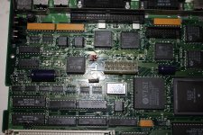
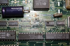
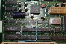
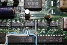
-
this board seems not to have any acid leak, and very little electrolyte damage.
-
the main problem is/was.......(and prob always will be) ue8
-
decided to start from scratch today. So removed all caps, ue8 and the pins from the cap legs I used last night
-
cleaned board
-
used very small wires to melt into via's around ue8 and then to solder onto ue8 legs/pins.
-
many pads and traces gone so hade to use wire
-
my problem (among others) is I just used basic continuity test on each pin on a good board to find any point where that pin would connect.
applied this to bad board
and soldered in the wires accordingly
-
still no joy
-
heres a few pics of where the board is, plus a short vid of what happens when I turn it on
-
and I know the wires are too dam big.............there all I could fine
-
weh hey!
the ue8 I am using was from a dead machine - are all these chips the same or is there different versions of a UE8 chip or does the big chunk of UE8 that I knocked off kinda upset the whole show?
-
cleaned ron and ram simms (I have 4 in it) with a rubber. Reseated the video memory chip
-
I removed UD8 during the cleaning to make sure the torn traces were not touching under the UD8.............they were not. When I went to put it back there was no writing on the chip to orientate it.......so I think I put it back the right way
-
helllppppppppppp
-
cleaned ron and ram simms (I have 4 in it) with a rubber. Reseated the video memory chip
-
I removed UD8 during the cleaning to make sure the torn traces were not touching under the UD8.............they were not. When I went to put it back there was no writing on the chip to orientate it.......so I think I put it back the right way
-
helllppppppppppp
You would be better off replacing those chips with new. I have a stash I ordered from digikey to do it. They are all the same. Well sorta.
There are HC, HCT, AS, F, variants, all with different speeds and voltage ratings. But otherwise thats about it.
In your neck of the woods, maybe Farnell carries them.
There are HC, HCT, AS, F, variants, all with different speeds and voltage ratings. But otherwise thats about it.
In your neck of the woods, maybe Farnell carries them.
don't know why my vids only show when you click on 'show all content' on the bottom of the screen techknight.
-
I have metered out all the connections and they are not shorting. they are all the same as the good board. But I am not using the schematic.
-
you say replace those chips.... as in all the video chips UA8 up to UG8...as in all 7 of them
I have another dead se30 ( I have 3 in total) and the ue8 has the numbers tif022 cr ls166a. All 7 are there... as in 1 set.
-
change them all?
-
I have metered out all the connections and they are not shorting. they are all the same as the good board. But I am not using the schematic.
-
you say replace those chips.... as in all the video chips UA8 up to UG8...as in all 7 of them
I have another dead se30 ( I have 3 in total) and the ue8 has the numbers tif022 cr ls166a. All 7 are there... as in 1 set.
-
change them all?
No... You want to replace UE8 with a brand new one, trust me.
With the horizontal line cutting in and out is a for sure bad connection, But replacing UE8 with a brand spanking new SN74LS166 would remove this factor out of the equation, so you dont have to keep mucking with it.
With the horizontal line cutting in and out is a for sure bad connection, But replacing UE8 with a brand spanking new SN74LS166 would remove this factor out of the equation, so you dont have to keep mucking with it.
we wouldn't have anything like that in Ireland techknight.
-
believe me this is one crap country for getting specific stuff. Everything is got online. So is a SN74LS166 some kind of generic chip that will definitely work as a UE8
-
been at this dam thing 4 hours now so feck it im off to bed. Gigging for the weekend so will have a stab at it on monday
-
cheers peoplez
-
believe me this is one crap country for getting specific stuff. Everything is got online. So is a SN74LS166 some kind of generic chip that will definitely work as a UE8
-
been at this dam thing 4 hours now so feck it im off to bed. Gigging for the weekend so will have a stab at it on monday
-
cheers peoplez
A question.
-
can an se/30 "single horizontal line" be caused by just UE8.?..........or can it be cause by any of the Ux8 chips (7 of them I think).....or anything else??
-
Display is perfect when I install my good board.
-
I have worked on the Ux8 chips, replaces the the FUJ2 258 chip, replaced both transistors next battery and crystal next battery - those parts were missing
Im running out of options
-
-
cheers people
-
can an se/30 "single horizontal line" be caused by just UE8.?..........or can it be cause by any of the Ux8 chips (7 of them I think).....or anything else??
-
Display is perfect when I install my good board.
-
I have worked on the Ux8 chips, replaces the the FUJ2 258 chip, replaced both transistors next battery and crystal next battery - those parts were missing
Im running out of options
-
-
cheers people
heres what I did tonight - took off UE8 and UC8 ( to find the via for one of the pins) - this exposed all the first via's , along the trace , to all the missing pads left
-
got smaller wire
-
finished it up ( no picture, time!) - but its still the same
-
will put up more pics tomorow
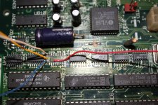
-
got smaller wire
-
finished it up ( no picture, time!) - but its still the same
-
will put up more pics tomorow
Techknight - went to swap out the PALS only to find they are all soldered into the board. Swapped out the video rom - still no joy.
-
heres where it is at now.
-
Id better get this going soon because the more I go at it the weaker all the connections, pads, traces are getting.
-
I have metered out the UE8 with my good board and it checks out...cleaned the boards both sides........I just cant find the fault...........it has to be something stupid.
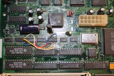
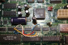
-
heres where it is at now.
-
Id better get this going soon because the more I go at it the weaker all the connections, pads, traces are getting.
-
I have metered out the UE8 with my good board and it checks out...cleaned the boards both sides........I just cant find the fault...........it has to be something stupid.
somebody gave this description in another post of same problem
"the Vertical Sweep IC at U2 (TDA1170A, 12-pin)"
-
what chip is that?..........I cant see a 12 pin chip on the se/30 board anywhere!............is this chip on the analog board?
-
I have metered out all the Ux8 chips and compared them to a good board. EVERY PIN IS CORRECT
-
is there anything else that's would cause the horizontal line.
-
would it be worth metering out all the pals
"the Vertical Sweep IC at U2 (TDA1170A, 12-pin)"
-
what chip is that?..........I cant see a 12 pin chip on the se/30 board anywhere!............is this chip on the analog board?
-
I have metered out all the Ux8 chips and compared them to a good board. EVERY PIN IS CORRECT
-
is there anything else that's would cause the horizontal line.
-
would it be worth metering out all the pals
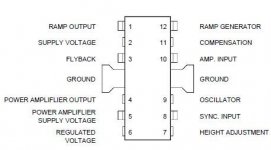
thanks 360alaska.
-
the analog board is good. When I swap in my good board display is perfect..............so its this darn motherboard.
-
I just cant find the problem and I cant hot air gun chips off anymore, the pads will all come off if I keep swapping chips
-
have to go on the assumption the chips are good
-
ah well..........off to a gig..........will spend hours staring at this thing later
-
the analog board is good. When I swap in my good board display is perfect..............so its this darn motherboard.
-
I just cant find the problem and I cant hot air gun chips off anymore, the pads will all come off if I keep swapping chips
-
have to go on the assumption the chips are good
-
ah well..........off to a gig..........will spend hours staring at this thing later
Well you need to look at the schematic. where is the vertical signal generated? the PALs I believe.
Even though they are soldered on, I would replace the one that is directly responsible for generating the vertical sweep drive.
Messing with UD8/UC8, etc all day isnt going to fix this problem I dont believe.
Even though they are soldered on, I would replace the one that is directly responsible for generating the vertical sweep drive.
Messing with UD8/UC8, etc all day isnt going to fix this problem I dont believe.
Alot of those suggestions come from here: http://www.biwa.ne.jp/~shamada/fullmac/repairEng.html
But of course, you know you analog board is good... Unless that board has a short somewhere that damaged U2, Unlikely though...
http://museum.dyne.org/gallery/apple/stuff/mac/andreas.kann/schemat.html
maybe this graphic i made will help you?
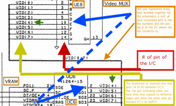
maybe this graphic i made will help you?
thanks uni - I looked at the drawing and understood nothing............then again im drunk as a lord - weh hey!
-
to be honest ive got to the stage where I must understand what is actually going on , on the board - what ALL the chips do etc etc
-
this is becoming an obsession.......just have to understand the board logic, use it to understand a problem, and again use it to find and fix the bas%$£d of a problem
-
It kills me not having the knowledge I need to understand this
-
off to utube for tutorials............god help me
-
thanks again all
-
to be honest ive got to the stage where I must understand what is actually going on , on the board - what ALL the chips do etc etc
-
this is becoming an obsession.......just have to understand the board logic, use it to understand a problem, and again use it to find and fix the bas%$£d of a problem
-
It kills me not having the knowledge I need to understand this
-
off to utube for tutorials............god help me
-
thanks again all
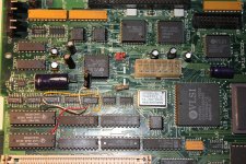
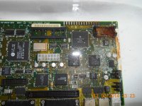
that's it for the 5 boards. The last remaining 2 boards (the CC and the classic) are just too far gone. The acid spill on the classic was a disaster. Rollermanz took a few pics before he did anything it.
-
look at how the metal frame 'melted'!!
-
the color classic........major damage, parts exploded/burnt!! ........even if I attemped to fix it, I was not going to try it im my machine.
-
so that's it. 5 boards and I got 2 working.
-
all good fun
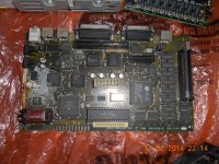
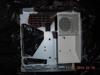
-
look at how the metal frame 'melted'!!
-
the color classic........major damage, parts exploded/burnt!! ........even if I attemped to fix it, I was not going to try it im my machine.
-
so that's it. 5 boards and I got 2 working.
-
all good fun