

Okay. Some of this may be a bit backwards, but I was able to trace through to what parts make up the floppy portion of the SE/30. Here it goes:
- J6 (external 19-pin connector) links up to F2 (fuse, 1A), C51 (capacitor, 0.01 mF? uF?), C52 (capacitor, same as C51), L16 (inductor, unknown value) and L17 (inductor, unknown value).
- J6 also links up with R30 (resistor, 22 K-ohm? 22-ohm?), C67 (33 pF), RP10 (Bourns network filter), J8 (internal floppy connector), L22 (inductor, unknown value), UJ11 (SWIM chip), L21 (inductor, unknown value), UI12 (53C80 SCSI Controller Chip), L8 through L10 (inductors, unknown value), C47 (capacitor, same value as C51), D3 (diode, 1N4001), F3 (fuse, 1A), J4 (External SCSI connector) and J5 (Internal SCSI connector).
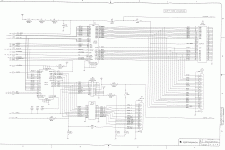
I've included a page of the schematic. I hope that's okay with the mods. If not feel free to omit. It was posted a while back to this site, so I figured it is safe to repost.
73s de Phreakout. :rambo:
- J6 (external 19-pin connector) links up to F2 (fuse, 1A), C51 (capacitor, 0.01 mF? uF?), C52 (capacitor, same as C51), L16 (inductor, unknown value) and L17 (inductor, unknown value).
- J6 also links up with R30 (resistor, 22 K-ohm? 22-ohm?), C67 (33 pF), RP10 (Bourns network filter), J8 (internal floppy connector), L22 (inductor, unknown value), UJ11 (SWIM chip), L21 (inductor, unknown value), UI12 (53C80 SCSI Controller Chip), L8 through L10 (inductors, unknown value), C47 (capacitor, same value as C51), D3 (diode, 1N4001), F3 (fuse, 1A), J4 (External SCSI connector) and J5 (Internal SCSI connector).
I've included a page of the schematic. I hope that's okay with the mods. If not feel free to omit. It was posted a while back to this site, so I figured it is safe to repost.
73s de Phreakout. :rambo: