

Thread
There're 8 RAM chips soldered to my Quadra 605's LB...
Could some appropriately skilled solder-jockey replace those 8 chips with, say, the 8 chips on this 32MB SIMM sitting in the slot next to them? (Actually now that I look closer, the number of pins on each chip on this SIMM is different than the chips on the LB, so that specific example wouldn't work.) Are there higher capacity chips that could be swapped in, to boost the total RAM available? I assume these are each 1MB chips, are there some 2MB or 4MB chips that are the same form factor?
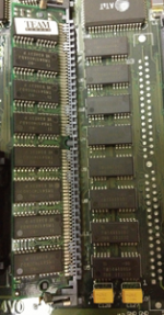
I don't think there would be any problems,
I am going to get my heat gun this weekend,
First i have to fix my se/30
once that is done, maybe same day?
I might start on the IIsi's ram.
I like the idea with the q605.
The IIsi is begging for this mod.
The LC-1 has empty spots ready for chips, (that one seams easy)
I am going to get my heat gun this weekend,
First i have to fix my se/30
once that is done, maybe same day?
I might start on the IIsi's ram.
I like the idea with the q605.
The IIsi is begging for this mod.
The LC-1 has empty spots ready for chips, (that one seams easy)
R&D precedes T&E . . . preferably. Check the Memory Map in the 475/605 DevNotes to see if there's any possibility of having hacked in RAM shoehorned in there. A machine with SIMM slots for Bank A will poll, test & map available memory. The startup routine of a soldered Bank A machine likely assumes, tests and maps only the standard allotment.
I'm hoping to be proved wrong. }
I'm hoping to be proved wrong. }
I am not aware of any ROM restrictions in this regard. The banks are dynamically sized. I'm not specifically familiar with the 605, since it is slightly different than the other djmemc controllers, but... There are 2 banks allocated for the soldered on memory. If you have the 605 with 4MB soldered, that's all in one bank. If you have the 605 with 8MB soldered, it's 4MB in each of the two banks, which means the banks are interleaved, resulting in about 10% or so faster memory accesses. So, if you're really trying to get the most out of your 605, make sure both banks are populated with the same memory.
In my head I was sure it was 8MB soldered on... so that makes it an even more enticing question.
@OOM actually I have two 605 boards and an internally blown up (courtesy of shoddy Spindler-plastic and the gentle ministrations of the USPS) 605 case that'll kind of stay together just by gravity holding everything in place, so the plan has been, for a while now, to have a Quadra Classic sitting next to its headless brother the Quadra 605. I just need to get one of them recapped, overclocked, and maybe (fingers crossed) memory bumped by Uniserver.
In its current SIMM + 4MB state it maxes out at 132MB. If it was a SIMM + 32MB (or more) that would be 28MB (or more) better, wouldn't it?
@OOM actually I have two 605 boards and an internally blown up (courtesy of shoddy Spindler-plastic and the gentle ministrations of the USPS) 605 case that'll kind of stay together just by gravity holding everything in place, so the plan has been, for a while now, to have a Quadra Classic sitting next to its headless brother the Quadra 605. I just need to get one of them recapped, overclocked, and maybe (fingers crossed) memory bumped by Uniserver.
In its current SIMM + 4MB state it maxes out at 132MB. If it was a SIMM + 32MB (or more) that would be 28MB (or more) better, wouldn't it?
Gotta leave for the baseball field in two minutes so this will be short.
Memory in the Q605 is 32 bits wide. If there are only eight chips, then they are 4 bits wide each or X4.
(1M X 4) X 8 chips yields 4 MB.
Memory of the requisite type comes as large as 16M X 4, but the chips are extra large. Look up the D4893 SIMMs on Ebay for a photo. Those are the largest capacity memory chips you can use. With those you can get 64MB into a 32 bit wide bank. But the connections would probably be a nightmare.
the 4M X 4 chips are about the same size, and if the pins match up and just tack on a couple at the end, then this would be much easier to connect. Just make a connection for the additional address lines from the SIMM socket. The address lines should be common and just the RAS and CAS lines unique between the sockets, I think. I'd want to test that with a DMM though to be sure. If the address lines aren't shared, you'll have to hunt down the extra lines on the controller chip, but it doesn't make any sense for them to duplicate address lines when they could share them.
4M X 4 chips will get you 16MB in a bank.
Rob, is there a software reason why the on-board RAM in the Q605 must be treated as single-banked? If there are four RAS lines to the on-board memory, the RAS signals might be handled in pairs by the controller, allowing the installation of two banks of memory by correct pairing of the RAS lines.
That's how the SIMM socket handles a 128MB or a 32MB SIMM. It has four RAS lines, but they're divided into two pairs and in a double banked SIMM, one bank uses one pair of RAS lines and the other bank uses the other pair. On a single banked SIMM I think either all four or just one pair are driven.
Memory in the Q605 is 32 bits wide. If there are only eight chips, then they are 4 bits wide each or X4.
(1M X 4) X 8 chips yields 4 MB.
Memory of the requisite type comes as large as 16M X 4, but the chips are extra large. Look up the D4893 SIMMs on Ebay for a photo. Those are the largest capacity memory chips you can use. With those you can get 64MB into a 32 bit wide bank. But the connections would probably be a nightmare.
the 4M X 4 chips are about the same size, and if the pins match up and just tack on a couple at the end, then this would be much easier to connect. Just make a connection for the additional address lines from the SIMM socket. The address lines should be common and just the RAS and CAS lines unique between the sockets, I think. I'd want to test that with a DMM though to be sure. If the address lines aren't shared, you'll have to hunt down the extra lines on the controller chip, but it doesn't make any sense for them to duplicate address lines when they could share them.
4M X 4 chips will get you 16MB in a bank.
Rob, is there a software reason why the on-board RAM in the Q605 must be treated as single-banked? If there are four RAS lines to the on-board memory, the RAS signals might be handled in pairs by the controller, allowing the installation of two banks of memory by correct pairing of the RAS lines.
That's how the SIMM socket handles a 128MB or a 32MB SIMM. It has four RAS lines, but they're divided into two pairs and in a double banked SIMM, one bank uses one pair of RAS lines and the other bank uses the other pair. On a single banked SIMM I think either all four or just one pair are driven.
There shouldn't be a software reason it's limited to 1 bank. If you were able to get the other lines and connect them to something, the ROM should find them just fine. The ROM doesn't hard code the sizes, it has a loop that iterates over all banks trying to figure out how big each bank is. So each bank is treated the same, whether it is soldered or socketed.
nope , after my luck with the LC-1, i decided to leave them be for the moment.
viewtopic.php?f=9&t=19776&p=188206#p188206
plus i have been super mega busy.
viewtopic.php?f=9&t=19776&p=188206#p188206
plus i have been super mega busy.