BIGMAC Pgmrs Model 8 85
BIGMAC Pgmrs Model 8 85
Macintosh · PDF
| Filename | BIGMAC_Pgmrs_Model_8-85.pdf |
|---|---|
| Size | 0.26 MB |
| Subsection | prototypes / 1985_Big_Mac |
| Downloads | 4 |
Enjoying MacTrove?
Anonymous downloads are free and unlimited.
Create a free account to track favorites,
contribute metadata corrections, and join the
community chat.
Reader
Loading…
OCR / Text contents
Rich Page
8/14/85
APPLE CONFIDENTIAL
Programmers Model for the Big Mac
Introduction
This document describes the Big Mac hardware from the programmers
view of the machine which includes a description of the address space
maps and a description of each device.
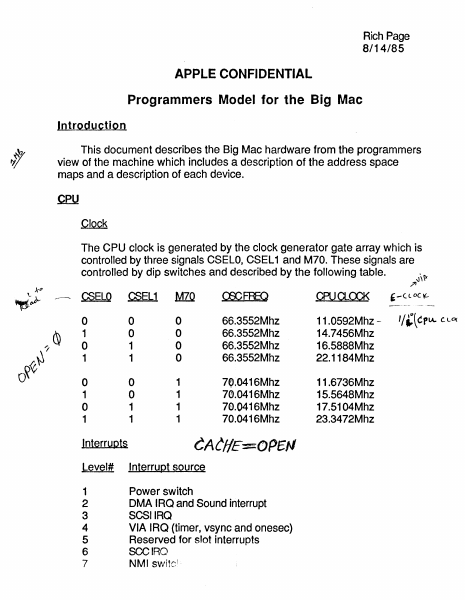
The CPU clock is generated by the clock generator gate array which is
controlled by three signals CSELO, CSEL 1 and M70. These signals are
controlled by dip switches and described by the following table.
x"
~ELQ
\.~
~
,~
/
rr}
O~
~EL1
MIQ
~FREQ
®a...CCK
0
1
0
1
0
0
1
1
0
0
0
0
66.3552Mhz
66.3552Mhz
66.3552Mhz
66.3552Mhz
11.0592Mhz 14.7456Mhz
16.5888Mhz
22.1184Mhz
0
1
0
1
0
0
1
1
1
1
1
1
70.0416Mhz
70.0416Mhz
70.0416Mhz
70.0416Mhz
11.6736Mhz
15.5648Mhz
17.5104Mhz
23.3472Mhz
CACHE:50PE#
lnterrupts
Level#
Interrupt source
1
2
3
4
5
Power sW'itch
DMA IRQ and Sound interrupt
SCSI IRQ
VIA IRQ (timer, vsync and onesec)
Reserved for slot interrupts
SCCIRO
NMI SVJitc
6
7
l
,
, - ( L DC \l.-
-_.
-~"--
..
__ ."-
'/~\CPlA. C.LD(
Rich Poge
8/14/85
Big Moe Address Spoce Mop (Supervisor Stet e)
--.
-
~
XXF9000 0
XXEOOOOO
XXDOOOOO
XXCOOOo"O
I/O
SLOTS
XXAOOOOO
XX900000
XX800000
XX700000
XX600000
XX500000
XX400000
XX300000
XX200000
XX100000
XXOOOOOO
XXFEOOOO
XXFDOOOO
MMU
ROM high
i
XXBOOOOO
XXFFOOOO
reserved
(" ""\
xx~pooo
XXFBOOOO
XXFAOOOO
XXF90000
reserved
---,-"--
DMA
VTG
----
IWM
VIA
SCC
RAM
RAM
RAM
RAM
RAM or ROM low
RAM
RAM
RAM
RAM or ROM zero
XXFOOOOO
--'-.---
SCSI
SCREEN
RAM
--
reserved
----
Rich Poge
8/14/85
Big Moe Address Spoce Mnp (User stote)
r
I/O
Frrooooo
FFFFOOOO
FFEOOOOO
DMA
MMU (no 6ccess)
FFCOOOOO
ROM high
-
VIA
FFFBOOOO
reserved
FFBOOOOO
...,,-----.-.---
-
FFF90000
SCC
,----==---
SCSI
_.
-
SCREEN
FF AOOODO
FFFOOOOO L
I
I
0070000 0 -
RAM
_.
RAM
00600000
-
RAM
00500000
RAM or ROM low
00400000
0030000'0
-,
IWM
FFFCOOOO
FFFAOOOO
-,
VTG
FFFDOOOO
FFDOOOOO
reserved
I-
FFFEOOOO
SLOTS
-
RAM
I-
00200000
00100000
00000000 I
-
RAM
RAM
RAM or ROM zero
...J
reserved
-
cpu (continued)
Bus Error
A bus error can be generated by either the AS watchdog or the MMU.
The AS watchdog will generate a bus error for bus cycles longer than
2us.
Hjgh Decode Map Register
There exists a 4 bit register (located on the VIA) which controls the
position of the ROM and provides a mechanism to limit the number of
address bits used for decoding logical addresses. This register can
\~~ programmed to cause the high address bits (those above A23) to be
significant to the decoding hardware. This allows a range of address
space sizes from 24 to 32 bits. In the smallest configuration, the
address space is limited to 16Mb and the upper eight bits are
insignificant to decoding which will allow software to use the upper
eight bits as tags. In the largest configuration, the address space is
4Gb and none of upper bits are available.
Address Space Map
The address space map is determined by the High Decode Map reg…
Showing first 3,000 characters of 6,366 total. Open the full document →