BIGMAC VTG
BIGMAC VTG
Macintosh · PDF
| Filename | BIGMAC_VTG.pdf |
|---|---|
| Size | 0.19 MB |
| Subsection | prototypes / 1985_Big_Mac |
| Downloads | 3 |
Enjoying MacTrove?
Anonymous downloads are free and unlimited.
Create a free account to track favorites,
contribute metadata corrections, and join the
community chat.
Reader
Loading…
OCR / Text contents
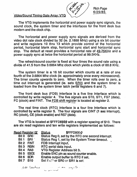
Rich Page
6/29/85
Yideo/Sound Timing Gate Array: VIG
The VTG implements the horizontal and power supply sync signals, the
sound clock, the system timer and the interfaces for the front desk bus
modem and the clock chip.
The horizontal and power supply sync signals are derived from the
video dot rate clock divided by 32 (ie. 2.1888 MHz) using a six bit counter
and write registers 10 thru 13 which provide control of the horizontal
period, horizontal blank stop, horizontal sync start and horizontal sync
stop. The default at reset provides a horizontal rate of 1!l.75KHz and a
power supply sync at twice the horizo~tal period at 99.5KHz.
The refresh/sound counter is fixed at four times the sound rate using a
divide of 41.5 from the 3.6864 Mhz clock which yields a clock of 88.8 KHz.
The system timer is a, 16 bit counter which counts at a rate of one
fourth of the 3.6864 Mhz clock (ie. approximately once every microsecond).
The timer counts upwards to zero. When the timer rolls over to zero, a
time out interrupt is generated (ie. s,ets ~ROJ and the system timer is
loaded from the the system timer latch (write registers 6 and 7).
The front desk bus (FOB) interface is a five line interface which is
controlled by write register 4. The five signals are STO, ST1, FS7 (data),
FC (clock) and FINT. The, FOB shift register
is located at register 2.
--===-;z
The real time clock (RTC) interface is a four line interface which is
controlled by write register 5. The four signals are CINT (1 sec interrupt),
RC (clock), CE (clock enable) and RS7 (data).
The VTG is located at $FFFOOP0~ with a register spacing of $10. There
are six read registers and ten write registers implemented as follows:
Bead Register 0: Status
$FFFOOOO 0
Bit 0 SRO
Status Reg 0, set by the RTC one second interrupt.
Bit 1 SR1 (
Status Reg 1, set by the System Timer timeout.
Bit 2 FINT
. FOB Interrupt input.
Bit 3 RSIN
RTC serial data input.
Bit 4 RA3
VTG Register Address bit 3 ..
Bit 5 ES:E
Enable ENC pin as sound counter enable.
Bit 6 ErA
Enable output buffer to RTC if set
Bit 7 S10
Set if er~her SRO orSR1 is set.
J
..-
17.-"\
Bead Register 2:
FDa Shifter
Beacf Begister 4:
Number..LQw
po~
$FFFk
1..0
This register allows the FOB shift register to be read.
$FFF~O
This register allows the low byte of the number register to be read.
Numberliigb
$FFFdbso tou"S1J
This register allows the high byte of the number register to be read.
Bead Register 5:
Read Register 6: Timer L~
$FFFD060
\?60 &0
This register allows the low byte of the sy~~em timer to be read.J7'~
Bead Register 7:
Timer Hlgh
$FFFD070
bClO 1 0
This register allows the high byte of the system timer to be read
V
,
Write Register 0;
Bit 0 SRO ,
Bit 1 SR1
Bit 4 RA3
Bit5 ~
Status
$FFFDOOOO
RTC one second interrupt bit.
System Timer timeout bit.
VTG Register Address bit 3.
Enable ENe pin as Sound Counter Enable.
Note: This register must be initialized at system reset.
The remaining bits should be zero when written.
$FFFOcfuO wit…
Showing first 3,000 characters of 5,035 total. Open the full document →