

Thread
Another IIci ROM hack
The IIsi dev notes page 74 says:
And indeed it does run! But the issues I ran into are: RocketWare apparently thinks the IIx is a IIsi and won't run, and the Minimal System installs for a IIx also don't run with the IIsi ROM. I haven't dug into it, but the Minimal System installs are apparently checking the machine time and (possibly) the revision byte, since changing both of those fool the min system.
bbraun, take a set of Quadra 950 ROMs and call me in the morning! [ ] ]'>
] ]'>
edit: I just waded through the last 20 pages/1,000 topics in the "all results" view of the "View active topics" list! 8-o
This introductory "IIci ROM hack" thread, the contributions of info and suggestions by many comrades . . . < gotta make a listing >
. . . and even the start of new, interrelated hack projects, such a bbraun's amazing ROM-Disk hack . . .
. . . have blown this thread right off the charts in just four months.
The only remaining topics with more posts/pages are the four years longer running:
Post your desktop on p.32 ATM . . .
. . . and What are you listening to? on p.31 as I type this!
What an amazingly Synergistic Hackin' Consortium :approve:
Thanks ever so much for joining us, dougg3, and for instigating all this fun! [ ] ]'>
] ]'>
] ]'>edit: I just waded through the last 20 pages/1,000 topics in the "all results" view of the "View active topics" list! 8-o
This introductory "IIci ROM hack" thread, the contributions of info and suggestions by many comrades . . . < gotta make a listing >
. . . and even the start of new, interrelated hack projects, such a bbraun's amazing ROM-Disk hack . . .
. . . have blown this thread right off the charts in just four months.
The only remaining topics with more posts/pages are the four years longer running:
Post your desktop on p.32 ATM . . .
. . . and What are you listening to? on p.31 as I type this!
What an amazingly Synergistic Hackin' Consortium :approve:
Thanks ever so much for joining us, dougg3, and for instigating all this fun! [
] ]'>
Q950 ROMs won't help the two problems I've mentioned, since the problems appear based on things checking the machine type & rom revision and making assumptions based on that. The "solution" is to modify those values in the ROM and hope for the best.
However, the newer the ROM, the larger it is generally speaking. The Q700 (all 040's?) and up ROMs are all 1MB. That's the entirety of mapped ROM space under older OS releases, so you don't have any space to play with. So, my general rule is: unless there's a specific reason to use a newer/larger ROM (such as 32bit cleanliness, faster ROM FPU routines, newer Something Manager releases, etc.), stick with the smallest ROM (typically the original shipping ROM for that system) to maximize the available space to play with.
For the moment, I'm using the stock IIx ROM just to minimize variables in my ROM disk hacking.
However, the newer the ROM, the larger it is generally speaking. The Q700 (all 040's?) and up ROMs are all 1MB. That's the entirety of mapped ROM space under older OS releases, so you don't have any space to play with. So, my general rule is: unless there's a specific reason to use a newer/larger ROM (such as 32bit cleanliness, faster ROM FPU routines, newer Something Manager releases, etc.), stick with the smallest ROM (typically the original shipping ROM for that system) to maximize the available space to play with.
For the moment, I'm using the stock IIx ROM just to minimize variables in my ROM disk hacking.
Good points, which brings up the question:
What benefit does the IIsi ROM give you over the Stock IIx ROM other than removing the requirement of running MODE 32? :?:
I'm beginning to wonder if I really need a newer ROM on my IIsi, given the statement in the DevNote and your experience with it in the IIx.
If I just add the extra Cards and the IIsi polls them at startup, I wonder if it will address more than the three PseudoSlot addresses specified?
If I hack the NuBus adapter's Slot ID, That ought to let me run the three spec'd addresses from cards in the subterranean expansion bay. }
What benefit does the IIsi ROM give you over the Stock IIx ROM other than removing the requirement of running MODE 32? :?:
I'm beginning to wonder if I really need a newer ROM on my IIsi, given the statement in the DevNote and your experience with it in the IIx.
If I just add the extra Cards and the IIsi polls them at startup, I wonder if it will address more than the three PseudoSlot addresses specified?
If I hack the NuBus adapter's Slot ID, That ought to let me run the three spec'd addresses from cards in the subterranean expansion bay. }
Here's the latest design. I found and fixed a few more stupid traces, cleaned up a lot of the traces so they look nicer when they go into IC contacts, added the jolly roger and used an LED for an eye, and that's about it.
I couldn't figure out how to import an EPS file into EAGLE, so I turned the Jolly Roger into a BMP and used its included BMP import script.
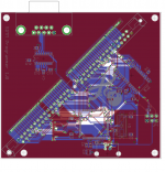
I couldn't figure out how to import an EPS file into EAGLE, so I turned the Jolly Roger into a BMP and used its included BMP import script.
With those SIP Headers, will it be possible to build a breadboard to program just about any ROM package?
Specifically, I'm thinking about hacked DuoDock & MiniDoc DeclROMs. On the other hand, updating the DeclROMs on Video Cards etc. that are long out of producyion from companies that no longer exist might be kinda nice too!
Specifically, I'm thinking about hacked DuoDock & MiniDoc DeclROMs. On the other hand, updating the DeclROMs on Video Cards etc. that are long out of producyion from companies that no longer exist might be kinda nice too!
Holy cow! I didn't see what you had written earlier until now. That's awesome! Thanks jt
It's been a blast and it continues to get even better as bbraun makes the SIMM contain a ROM disk. Who knows what other possibilities are in store for this thread... Yep! I do believe so. Except for the VCC/GND pins, each one of those pins is pretty much its own IO pin connected to either the microcontroller or the IO expander. So as long as the ROMs do not need a higher Vpp voltage for programming, and they have fewer than however many pins I have going into it, we could definitely add a connection to it. (And it would take firmware support for that chip, of course...)
I've started writing some of the basic drivers for the programmer board already, even though I don't have a board or CPU on hand. Just getting familiar with the IO expander IC and how read/write cycles work on the Flash chips...
Also found a little bug on the board already. Glad I haven't had any manufactured yet. The pullup resistor on the IO expander chip's /RESET pin should be a pulldown resistor, keeping it in reset until I tell it to go out of reset. It's there because the AVR ISP programming also uses the SPI bus, and I'd like the IO expander chip to butt out while I'm programming the AVR
JT, the interrupt for each slot has support in hardware. So even though all the ROMs for both three and six slot models may have code to poll six slots when an interrupt occurs, the interrupt signal line(s) from the slot need to be connected properly.
I don't know how the 68030 models handle the hardware end -- I think it involves the VIA registers -- but in the PowerMac x500 models, the Grand Central chip has a pin for each interrupt and the interrupt wire from each PCI slot must be connected to a unique interrupt pin on Grand Central. Since the PCI slot IDs are coded into the ROM/Open Firmware Device Tree in those models, I suspect that the interrupt used needs to match the PCI slot address.
Anyway, the point is, that expanding the number of slots supported goes beyond providing support in the ROM and hooking up the expansion bus. The interrupt line connection can be pretty complicated.
I don't know how the 68030 models handle the hardware end -- I think it involves the VIA registers -- but in the PowerMac x500 models, the Grand Central chip has a pin for each interrupt and the interrupt wire from each PCI slot must be connected to a unique interrupt pin on Grand Central. Since the PCI slot IDs are coded into the ROM/Open Firmware Device Tree in those models, I suspect that the interrupt used needs to match the PCI slot address.
Anyway, the point is, that expanding the number of slots supported goes beyond providing support in the ROM and hooking up the expansion bus. The interrupt line connection can be pretty complicated.
dougg3,
It looks to me that some work still needs to be done around IC2 (SOIC package?).
What is your setting for copper pour back-off or something? I would increase it a bit.
It all depends, of course, how good your PCB manufacturer is. If the traces are too close to each other or too close to large copper areas, shorts might develop. (been there)
What colors represent which layer, btw?
It looks to me that some work still needs to be done around IC2 (SOIC package?).
What is your setting for copper pour back-off or something? I would increase it a bit.
It all depends, of course, how good your PCB manufacturer is. If the traces are too close to each other or too close to large copper areas, shorts might develop. (been there)
What colors represent which layer, btw?
I'll see what I can do with some of the traces on IC2...thanks!
You're right, I had the copper pour isolation set too low. I upped it to 12 mils or so, but now I'm running into problems with my ground planes disconnecting from each other. So I have some issues to solve there...
Red is the top layer. It's VCC except for the section surrounding the crystal, which is ground. Blue is the bottom layer and it has a ground fill.
You're right, I had the copper pour isolation set too low. I upped it to 12 mils or so, but now I'm running into problems with my ground planes disconnecting from each other. So I have some issues to solve there...
Red is the top layer. It's VCC except for the section surrounding the crystal, which is ground. Blue is the bottom layer and it has a ground fill.
dougg3, you mean the whole top layer is connected to + 5V? Not that it's wrong.... it's rather unusual. Normally one dedicates the whole layer to VCC when there are 3 or more layers available.
When there are only two layers availble I usually route +VCC as traces, dedicate one side to GND and connect all large copper islands on the other side to GND with several vias evenly spread around that copper island. That's when working with clock rates up to 25 MHz.
P.S. I know, giving advice is soo easy... Good luck!
When there are only two layers availble I usually route +VCC as traces, dedicate one side to GND and connect all large copper islands on the other side to GND with several vias evenly spread around that copper island. That's when working with clock rates up to 25 MHz.
P.S. I know, giving advice is soo easy...
Good luck!
Yes, exactly, ojfd. Everywhere you see big red areas (except around the crystal) its connected to +5V. I do have thick +5V traces routed to everywhere inside the copper fill (the copper fill just covers them up), so it won't be a big deal to change the top copper fill to GND if needed.
I guess I was under the impression that a ground pour on one side and a VCC pour on the other side was common. I'm definitely not opposed to changing it so the top is ground too though I'm new to this PCB design stuff so I appreciate the help from more experienced people such as you
Would you mind looking at my +5V traces after I change the copper fill? I'm a little worried because I have no idea what I'm doing when I route the +5V traces and the copper pour kind of masked my concerns for example, does it matter how I do the traces as long as they are thick and touch each part that they are supposed to touch? Or are there more complicated rules about how they are supposed to be connected?
Thanks for all the tips/suggestions you've been giving me!
I guess I was under the impression that a ground pour on one side and a VCC pour on the other side was common. I'm definitely not opposed to changing it so the top is ground too though
I'm new to this PCB design stuff so I appreciate the help from more experienced people such as you Would you mind looking at my +5V traces after I change the copper fill? I'm a little worried because I have no idea what I'm doing when I route the +5V traces and the copper pour kind of masked my concerns
for example, does it matter how I do the traces as long as they are thick and touch each part that they are supposed to touch? Or are there more complicated rules about how they are supposed to be connected?Thanks for all the tips/suggestions you've been giving me!
No problem, but try not to overdo your design, if it works, then it is ok as it is.
I just thought that, if you route your VCC as traces and leave GND issues out for a moment it might turn out as simpler design.
There are some, but I don't think these apply to your board. I'll see what papers on this subject I can dig up.( if I could only remember their names and where they are...)
One good idea is to separate ICs by using ferrite beads in their VCC lines and capacitors to GND after them. As bonus you gain space underneath those beads to route traces there, in cace where they will otherwise cross. I also don't see any larger (10uF +) filtering caps on your board. At least one would be good to buffer VCC that's coming from USB. SMD or 'thru hole', whatewer works.
EDIT - here's one by respectful Dutch engineer who also deals with mixed signal stuff, just like me:
http://www.tentlabs.com/InfoSupport/Technology/page35/files/Supply_decoupling.pdf
Quote from that paper:
I knew, it was something like that, nice to have it confirmed by someone else. But as I said before, it might work OK on your board, so don't worry too much about it
EDIT 2 - see end of the paper Appendix 1:
http://www.micrel.com/_PDF/HBW/App-Notes/an-01.pdf
dougg3, to confuse you even further, here are some more papers on power supply bypassing.
http://www.ti.com/lit/an/scaa048/scaa048.pdf
http://www.ti.com/lit/an/scba007a/scba007a.pdf
but that's ENOUGH!
TIP: try using different size of capacitors - i.e.1206 instead of 0805 if you need space to route trace underneath them. Ferrite beads could be1806 or even 'thru hole'.
http://www.ti.com/lit/an/scaa048/scaa048.pdf
http://www.ti.com/lit/an/scba007a/scba007a.pdf
but that's ENOUGH!
TIP: try using different size of capacitors - i.e.1206 instead of 0805 if you need space to route trace underneath them. Ferrite beads could be1806 or even 'thru hole'.
That's good info! I've made several custom PCBs over the past two years, all of them with GND and VCC pour on the top and bottom like Doug did, just because that's what seemed intuitive to me. But I don't have any formal training in PCB layout, and have just been winging it. I wish there were some kind of "PCB layout for Dummies" to learn from. I've been adding bypass capacitors, and trying to minimize trace lengths, but otherwise it's all just seat of the pants engineering. Fortunately everything I've designed so far has worked.
p.23 & gaining!
I was ASSuMEing that the NuBus Bridge Chipset handled the Two Slot (DuoDock's Gemini Slot Splitter Card w/Slot Assignments ____ and ___ ), Three Slot & Six Slot NuBus implementations, which are ASSuMEdly Buffered by that ChipSet from the rest of the I/O structure of the Mac Hardware.
The evidence that leads me to that conclusion would be that the NuBus Slots on the DuoDock remain active even with the Dock's DeclROM removed/disabled. In this configuration, all related Dock Services (and all the Dock's remaining circuitry?) are disabled. This was the basis for my plans to create the NuBusMiniDock™ hack for the DuoBoomBoxDock™ hack back in the day. There was a prize of a Mac offered by ________________ , one of the mods over on 'fritter, for the first one to hack some kind of Stereo System ten or so years ago.
The DuoDock Gemini Card uses the same _________________ Chipset as the IIsi's NuBus adapter, while the Dock+ uses the NuChip (____?____) Bridge Chipset, not that that matters. Considering that the Expanse Boxes made it possible to use extra PseudoSlot (my guess) NuBus IDs to be addressed by the Mac, I was hoping that a Six Slot ROM would Make the Extra IDs available in Firmware, while changing the NuBus Slot ID glue on the IIsi's NuBus adapter would give me a fourth PseudoSlot (NuBus) ID freeing up the IIsi's PseusoSlot ____ for Three PDS Card/NuBus slung underneath the MoBo, addressed in the IIsi's stock Memory Map. That, along with allowing a full compliment of RAM to be addressed in the unbuffered Bank A.
No Video Sense Lines/Cable polled on the Vampire Video Connector at startup = No buffer enable = freeing up the "normally" buffered Bank A for HACKING . . . }
. . . maybe! : It seems as though I've gotta study a bunch of Block Diagrams again . . . :-/
. . . not to mention the NuBus Spec for identifying the digital glue that determines the Slot ID! FEH!
Let me know if you think I'm heading for a dead end or three!
Thanks to ojfd's help in my IIfx/CD 5 year tune-up . . . thread, I've now got a chance to determine new info on Slot Id's! [] ]'>

< . . . reminds self to change name of thread to ___ & NuBus Card Madness or some such . . . >
__________________________________________________
I'll edit in all the blanks left for Slot IDs, Chipset and ASIC info when I get a chance.
Thanks for the informed input, trag. Your mastery of hardware/firmware is much envied by this technically untrained comrade. :approve:
I was ASSuMEing that the NuBus Bridge Chipset handled the Two Slot (DuoDock's Gemini Slot Splitter Card w/Slot Assignments ____ and ___ ), Three Slot & Six Slot NuBus implementations, which are ASSuMEdly Buffered by that ChipSet from the rest of the I/O structure of the Mac Hardware.
The evidence that leads me to that conclusion would be that the NuBus Slots on the DuoDock remain active even with the Dock's DeclROM removed/disabled. In this configuration, all related Dock Services (and all the Dock's remaining circuitry?) are disabled. This was the basis for my plans to create the NuBusMiniDock™ hack for the DuoBoomBoxDock™ hack back in the day. There was a prize of a Mac offered by ________________ , one of the mods over on 'fritter, for the first one to hack some kind of Stereo System ten or so years ago.
The DuoDock Gemini Card uses the same _________________ Chipset as the IIsi's NuBus adapter, while the Dock+ uses the NuChip (____?____) Bridge Chipset, not that that matters. Considering that the Expanse Boxes made it possible to use extra PseudoSlot (my guess) NuBus IDs to be addressed by the Mac, I was hoping that a Six Slot ROM would Make the Extra IDs available in Firmware, while changing the NuBus Slot ID glue on the IIsi's NuBus adapter would give me a fourth PseudoSlot (NuBus) ID freeing up the IIsi's PseusoSlot ____ for Three PDS Card/NuBus slung underneath the MoBo, addressed in the IIsi's stock Memory Map. That, along with allowing a full compliment of RAM to be addressed in the unbuffered Bank A.
No Video Sense Lines/Cable polled on the Vampire Video Connector at startup = No buffer enable = freeing up the "normally" buffered Bank A for HACKING . . . }
. . . maybe! :
It seems as though I've gotta study a bunch of Block Diagrams again . . . :-/ . . . not to mention the NuBus Spec for identifying the digital glue that determines the Slot ID! FEH!
Let me know if you think I'm heading for a dead end or three!
Thanks to ojfd's help in my IIfx/CD 5 year tune-up . . . thread, I've now got a chance to determine new info on Slot Id's! [
] ]'>< . . . reminds self to change name of thread to ___ & NuBus Card Madness or some such . . . >
__________________________________________________
I'll edit in all the blanks left for Slot IDs, Chipset and ASIC info when I get a chance.
Hey ojfd, thanks for all the detailed info! Wow! I really appreciate all of the info you dug up. I didn't even think about the benefits for routing by creating places that can be crossed. I saw that ferrite beads are a good idea (I think in the AVR documentation?) but I have been skipping them because I wasn't sure if they mattered for my application. If I added beads to my microcontroller would I need a different set of them for each VCC/GND pair on the microcontroller?
I actually do have a 10uF capacitor just to the right of the USB connector, on the bottom side of the board. I actually read that the value of that capacitor should not be any bigger than 10uF for USB (otherwise you get too much inrush current when it's first plugged in?).
OK, thanks! This is really good info to knowI knew, it was something like that, nice to have it confirmed by someone else. But as I said before, it might work OK on your board, so don't worry too much about it
I am using smaller bypass capacitors (particularly on the microcontroller) because the bigger they are, the more routing space they take up, making it harder to route the traces for pins directly next to the VCC/GND pins.
Haha, exactly! I'm in the exact same boat. I'd love to read a book like that too. The whole PCB layout is a lot tougher than it sounds. I have a lot of respect for people who design PCBs!I wish there were some kind of "PCB layout for Dummies" to learn from. I've been adding bypass capacitors, and trying to minimize trace lengths, but otherwise it's all just seat of the pants engineering. Fortunately everything I've designed so far has worked.
Edit: Here is what the PCB looks like with VCC as traces. All of the copper pours are GND. I have highlighted VCC so it's easy to see:
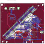
I had some isolated areas that didn't have a fill before, near the middle of the board. Some of them overlapped with areas on the other layer that did have ground available, so I used vias to connect them and fill in the empty spaces. In some cases, this new fill then overlapped with an empty area on the other layer, so I added yet another via, and now a bunch more of the board has a copper pour. Is this OK/advisable to do, or am I creating some kind of crazy antenna or RF emitting?
Or does it not matter at all?
Hey, guys, RELAX! As long as you don't have to deal with high clock rates, transmission lines, ground bounce, mixed signal, clock coupling into sensitive analog nodes, thermal drift and all that sort of stuff, I think your boards will work just fine the way you've designed them and it will not matter whether they have power plane or not.
And, btw, I have great respect for you, programmers. That stuff is mostly double dutch to me (although I've been successfull with ResEdit on a couple of occasions ;-) )
And, btw, I have great respect for you, programmers. That stuff is mostly double dutch to me (although I've been successfull with ResEdit on a couple of occasions ;-) )
It is OK - I would do it. I come from school where more ground is always good, but, as I've said before, it might not matter at all in your particular caseIs this OK/advisable to do, or am I creating some kind of crazy antenna or RF emitting?
it not matter at all?
Board looks nice, btw.
Thanks ojfd!
Now I'm busy separating the traces from each other a bit. I just realized my design rule check was set at 6 mils for clearance. Seeed Studio claims they can do it, but I don't trust that they will be able to do it reliably. I'm trying to get 8 mils of clearance at minimum...
Now I'm busy separating the traces from each other a bit. I just realized my design rule check was set at 6 mils for clearance. Seeed Studio claims they can do it, but I don't trust that they will be able to do it reliably. I'm trying to get 8 mils of clearance at minimum...
I worked a few tricks I've learned over the years doing analog photography.
Basically, I hoodwinked my very first digital camera into taking some halfway decent pictures of the Jolly Roger in action! :approve:
IIsiHackKluge:

Close-up of the Rev.1 Jolly Roger in action:

p.s. Tweaking in GraphicConverter helps a lot, but there's NOTHING like dodgin'-n-burnin' print effects in an analog darkroom! }
Basically, I hoodwinked my very first digital camera into taking some halfway decent pictures of the Jolly Roger in action! :approve:
IIsiHackKluge:
Close-up of the Rev.1 Jolly Roger in action:
p.s. Tweaking in GraphicConverter helps a lot, but there's NOTHING like dodgin'-n-burnin' print effects in an analog darkroom! }
Very nice jt! It's awesome to see the Jolly Roger happy inside a Mac! Cool pics!Latest update: I have a headache now, but 400+ DRC errors fixed later, I now have a board that passes the test with 8 mil spacing...
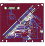
I think I'm going to pass on the ferrite beads on this board, but I'll definitely keep them in mind in the future (or if I start having hardware problems...)
Thanks, doug! Although, at this point, I think I'd describe it more as the Jolly Roger resigned to being in the middle of a Mess! :lol:
BTW, I discovered something quite by accident while I was taking those shots. When there's no monitor attached to the MoBo and no Monitor attached to the Liberty Adapter for the Radius Color Pivot II/IIsi Card, I get a five note death chime a few seconds after the boot chime every time! Plug in the 16" Sony Trinitron to power up the sense lines on the IIsi's MoBo and it boots up like a champ.
The results are repeatable, therefore I just have to test it out with the MoBo ROM and both the IIsi ROM SIMM configurations to see what's up. :?:
Simply maaaaaahvelous! :
Though it normally ROCKS, serendipity apparently gots its compliment of Yang to balance the Yin . . . like everything else!
__________________________________________________________
I just had a thought about the placement of your header rows . . . for clearance . . .
. . . how complicated would it be to move them another 10-15 mills farther from the SIMM Socket?
BTW, I discovered something quite by accident while I was taking those shots. When there's no monitor attached to the MoBo and no Monitor attached to the Liberty Adapter for the Radius Color Pivot II/IIsi Card, I get a five note death chime a few seconds after the boot chime every time! Plug in the 16" Sony Trinitron to power up the sense lines on the IIsi's MoBo and it boots up like a champ.
The results are repeatable, therefore I just have to test it out with the MoBo ROM and both the IIsi ROM SIMM configurations to see what's up. :?:
Simply maaaaaahvelous! :
Though it normally ROCKS, serendipity apparently gots its compliment of Yang to balance the Yin . . . like everything else!
__________________________________________________________
I just had a thought about the placement of your header rows . . . for clearance . . .
. . . how complicated would it be to move them another 10-15 mills farther from the SIMM Socket?
Interesting! I don't think that would matter as far as the SIMM is concerned, but I guess it depends on which ROM image you're booting from.
It is definitely possible to move the headers for some clearance. Good idea--there's plenty of board space available, even more if I move the RS-232 chip up. I'll do that! Shouldn't be a difficult change.
It is definitely possible to move the headers for some clearance. Good idea--there's plenty of board space available, even more if I move the RS-232 chip up. I'll do that! Shouldn't be a difficult change.
Moved it back as far as I could with the size of the board being what it is...sorry if these PCB design updates are getting annoying, I'm almost done!
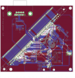
Congratulations, dougg3, very nice job! Fixing 400+ errors manually indeed takes some time.I have a headache now, but 400+ DRC errors fixed later, I now have a board that passes the test with 8 mil spacing...
Yes, skip them. I am 100% sure that your board will work as it stands now.
I thin'k it's very good and very educational to that you're publishing progress of your design, especially for casual reader. Next time people, who thought that it's all automatic, 5 minutes, auto-router does it all, will (hopefully) aprreciate the amount of work needed to create a finished product and (hopefully) will stop whining when asked to pay fair price for it.
Go dougg3!
I'll second that motion, I think it's great that you're documenting the process of creating, not just grounbreaking 68k firmware hacking, but the actual hardware to make it practical for others to try, and now, the tools required to get involved for others to play around with old Macs at an affordable price.
I'm continually amazed at your three level hacking thread, bbraun's incredible ROM Expansion achievements and all the technical expertise you've brought out of the woodwork from so many comrades. The tangential projects under development, like BMOWs unprecedented work and his involvement here in this thread, have been a boon to all.
Your introductory thread has become a treasure trove of content and demolished windmills, DQ!
Go, doug, go!**
jt
p.s. you moved the headers much farther back, great job. I've got pictures of triangular adapter cards dancing around in my head! :approve:
** silly literary reference for anybody who's read to kids )
)
I'm continually amazed at your three level hacking thread, bbraun's incredible ROM Expansion achievements and all the technical expertise you've brought out of the woodwork from so many comrades. The tangential projects under development, like BMOWs unprecedented work and his involvement here in this thread, have been a boon to all.
Your introductory thread has become a treasure trove of content and demolished windmills, DQ!
Go, doug, go!**
jt
p.s. you moved the headers much farther back, great job. I've got pictures of triangular adapter cards dancing around in my head! :approve:
** silly literary reference for anybody who's read to kids
) Thanks!!! It took a ridiculous amount of time
Although sometimes fixing one error would make 10 of the DRC errors go away, but still...it was ridiculous. I think if I had set the auto router correctly for 8 mil spacing I would have been better off. I agree totally with what you said. The auto router is nice but you really have to do a lot of cleanup by hand, and it ain't easy!I thin'k it's very good and very educational to that you're publishing progress of your design, especially for casual reader....
Go dougg3!
Thanks guys! I appreciate all the help and suggestions and everything. This has been a cool way for me to learn a lot about hardware
Not to mention I'm incredibly impressed by all the other cool stuff that has happened in here, like olePigeon's graphics and bbraun's ROM disk!LOL...or for anyone who has ever been a kidI've got pictures of triangular adapter cards dancing around in my head! :approve:
** silly literary reference for anybody who's read to kids
OK, so here's the deal. I think I'm pretty much done with the board. I added a few labels for the pin numbers and stuff. I'll still go over the layout and schematic with a fine-toothed comb a few more times, but it's pretty much done. In celebration, I used a cool script for EAGLE to render an (almost assembled) PCB in 3D! (Sadly, I don't think it has a 3D model of the SIMM socket)
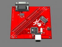
Go, Dawg, GO! VERY, VERY 
That rendering is beeeaaaaauuuuutifuuuuul! :approve:
Now that I've seen the connectors and header pins, I've got a couple of packaging considerations for you. :
If there's any way to move the USB connector over so that it hangs over the edge just about the thickness of a piece of thin plexi (actual thickness to be determined) and the DB-9 out to just about the same amount, I can see your board enclosed in a clear box with a clear plexi hinged lid or a rabbeted pop-top!
I know the crystal can positioning may be problematic, doug, but it might be worth a bit of rework. Some metal screening material inside the plexi for RFI reduction purposes and ESD event prevention might push the packaging parameters out a little farther than I first thought.
ojfd, what do you think? :?:
edit: a bent or mitered aluminum angle exoskeleton with a rabbeted clear plexi pop top and clear fixed base plate/chassis might be better!
That rendering is beeeaaaaauuuuutifuuuuul! :approve:
Now that I've seen the connectors and header pins, I've got a couple of packaging considerations for you. :
If there's any way to move the USB connector over so that it hangs over the edge just about the thickness of a piece of thin plexi (actual thickness to be determined) and the DB-9 out to just about the same amount, I can see your board enclosed in a clear box with a clear plexi hinged lid or a rabbeted pop-top!
I know the crystal can positioning may be problematic, doug, but it might be worth a bit of rework. Some metal screening material inside the plexi for RFI reduction purposes and ESD event prevention might push the packaging parameters out a little farther than I first thought.
ojfd, what do you think? :?:
edit: a bent or mitered aluminum angle exoskeleton with a rabbeted clear plexi pop top and clear fixed base plate/chassis might be better!
I can't speak for dougg3, but for me that would mean total re-design. Time=$, you know.
Besides, you can make your plexi box just a tad larger than PCB, so that USB and DB-9 will line up with the outer surface of the walls nicely and it will look just fine. Others might want to put the PCB in different box and they might have different opinions about preferred look of the final product.
Just let the dougg3 do his job and finish his PCB.
Otherwise, you know what they say about the camel? It is a horse designed by the committee. [
] ]'>