

Thread
Another IIci ROM hack
Optimizing routing by hand is why we have PCB designers. If hardware/software were to come anywhere near the complexity of the wetware between your ears, we'd be looking at a whole new world.
We're a lonnnngggg way from the likes of Commander Data . . . or even something as simple as deh Terminator. 8-o
I think maybe we're overlooking a simple solution by focusing on the Mac's provision for PDS I/O.
 ] ]'>
] ]'>
I've got a significant quantity of DPST DIP Switches on hand which would make for a more elegant solution than my DuoDock DeclROM power pin hack. [ ] ]'>
] ]'>

edit: WOOHOO!!!!!!!!!!!!!!! p.31 :approve:
We're a lonnnngggg way from the likes of Commander Data . . . or even something as simple as deh Terminator. 8-o
I think maybe we're overlooking a simple solution by focusing on the Mac's provision for PDS I/O.
An actual 72 pin RAM SIMM Saver knock-off may be a more elegant approach. Design a simple Card with a slot for the displaced RAM SIMM as close to the MoBo as possible and a slot or more for the standard ROM SIMMs above it would open the likes of the MicroQuadra 605, the Quadra 630 and all its ROM SIMM socket deprived offspring to ROM SIMM playtime. [
] ]'>I've got a significant quantity of DPST DIP Switches on hand which would make for a more elegant solution than my DuoDock DeclROM power pin hack. [
] ]'>
edit: WOOHOO!!!!!!!!!!!!!!! p.31 :approve:
Wow, a lot of crazy ideas floating around here. 
Some kind of PDS hardware for the future sounds really cool- all the different flavors of PDS out there is a bummer though.
Sounds like you're on a good approach, keep it simple for fewer headaches in the future. I guess I'll float another suggestion, how about a new color for the new PCB?
Some kind of PDS hardware for the future sounds really cool- all the different flavors of PDS out there is a bummer though.
A 72 pin RAM SIMM adapter neatly side-steps the Slots of Babel issue. On the MicroQuadras, the 630 and others, disabling the MoBo RAM and jumpering its RAS/Bank select lines to the adapter would allow for TWO RAM SIMM Slots to be active along with a set of ROM SIMMs. [ ] ]'>
] ]'>
] ]'>
This RAM/ROM PDS board is a really cool idea jt, and if it works it could certainly integrate all sorts of other upgrades into the future through more revisions.
It worries me that the address lines of ROM are not continuous with the address lines of RAM in the Mac IIci as seen here. It could be something complicated like a RAM controller on the logic board, or something as simple as buffers somewhere on the logic board that make the test fail, so this may be a non-issue, I don't know. For sure, we would need to know how the Mac determines how much RAM is installed. That would tell us a lot.
If it's possible to add RAM via PDS, I don't see any particular reason why we couldn't integrate a modern RAM module slot and fill that baby with a huge module (say 128MB :lol: ), that would be cool.
It worries me that the address lines of ROM are not continuous with the address lines of RAM in the Mac IIci as seen here. It could be something complicated like a RAM controller on the logic board, or something as simple as buffers somewhere on the logic board that make the test fail, so this may be a non-issue, I don't know. For sure, we would need to know how the Mac determines how much RAM is installed. That would tell us a lot.
If it's possible to add RAM via PDS, I don't see any particular reason why we couldn't integrate a modern RAM module slot and fill that baby with a huge module (say 128MB :lol: ), that would be cool.
THX, Dennis, I'm glad you mentioned the SIMM Saver, that's what gave me the notion for the 72 pin RAM/ROM adapter SIMM. [] ]'>
I'm pretty sure that the problems in the IIci have to do with it being saddled with 30 pin SIMMs and Bank A being buffered for Vampire Video. The ROM SIMM probably has something like two or four times the data lines of a 30 pin RAM SIMM. Dunno offhand, but the IIci already has a SIMM Slot available, like most of the 030 Macs.
The 72 pin RAM SIMM wedge for the ROM SIMMs would be aimed at systems with unimplemented pads (or no pads at all?) for a ROM SIMM that are saddled with PDS Slots of Babel, like the systems I mentioned.
] ]'>I'm pretty sure that the problems in the IIci have to do with it being saddled with 30 pin SIMMs and Bank A being buffered for Vampire Video. The ROM SIMM probably has something like two or four times the data lines of a 30 pin RAM SIMM. Dunno offhand, but the IIci already has a SIMM Slot available, like most of the 030 Macs.
The 72 pin RAM SIMM wedge for the ROM SIMMs would be aimed at systems with unimplemented pads (or no pads at all?) for a ROM SIMM that are saddled with PDS Slots of Babel, like the systems I mentioned.
So just so I get this straight, are you guys talking about making something that plugs into a RAM SIMM slot and patches new ROM into it? Does that even work? At least on the IIci, they're all mapped into different spaces physically by the circuitry. The address lines in the ROM SIMM sockets only do ROM addresses. The address lines on the RAM SIMM sockets only do RAM addresses. I could be totally misreading what you guys are talking about though, so forgive me if I'm confused!
As far as the 8 MB ROM SIMM goes, after a few failed auto-route attempts where the failed traces were pretty much impossible to route, I did what I should have done originally. I moved the chips so I now have them in sets of two. The advantage here is the data pins on the chips are now very close to the corresponding SIMM contacts. This opens up much more room for the address lines to be routed. Then I manually routed the VCC traces and data lines before doing the autorouter. This time the autorouter succeeded at routing everything else! I have a TON of cleanup work to do and I will do a lot of manual trace fixing now that the autoroute is complete. So, lesson learned: good placement of components on the PCB is a big deal!
I've got a ground copper pour on the top and bottom of the SIMM. I've connected the top and bottom pours together in multiple places to increase coverage over the whole SIMM and it's looking pretty good Red is the top layer, blue is the bottom layer. If I can, I'd like to increase the copper pour's coverage even more during the trace fix-ups; we'll see what I can do! The picture below is just what the autorouter spit out combined with extra vias I added, and as you can see it's a mess!
I've ditched the small 64-pin header to make more space; thanks to olePigeon, I pretty much have a lifetime supply of 64-pin SIMM sockets.
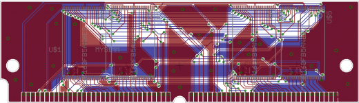
At least on the IIci, they're all mapped into different spaces physically by the circuitry. The address lines in the ROM SIMM sockets only do ROM addresses. The address lines on the RAM SIMM sockets only do RAM addresses. I could be totally misreading what you guys are talking about though, so forgive me if I'm confused!As far as the 8 MB ROM SIMM goes, after a few failed auto-route attempts where the failed traces were pretty much impossible to route, I did what I should have done originally. I moved the chips so I now have them in sets of two. The advantage here is the data pins on the chips are now very close to the corresponding SIMM contacts. This opens up much more room for the address lines to be routed. Then I manually routed the VCC traces and data lines before doing the autorouter. This time the autorouter succeeded at routing everything else! I have a TON of cleanup work to do and I will do a lot of manual trace fixing now that the autoroute is complete. So, lesson learned: good placement of components on the PCB is a big deal!
I've got a ground copper pour on the top and bottom of the SIMM. I've connected the top and bottom pours together in multiple places to increase coverage over the whole SIMM and it's looking pretty good
Red is the top layer, blue is the bottom layer. If I can, I'd like to increase the copper pour's coverage even more during the trace fix-ups; we'll see what I can do! The picture below is just what the autorouter spit out combined with extra vias I added, and as you can see it's a mess!I've ditched the small 64-pin header to make more space; thanks to olePigeon, I pretty much have a lifetime supply of 64-pin SIMM sockets.
Despite the need for optimization, that's a nice lookin' board layout! :approve:
I haven't had a IIci in hand for a almost a decade, so I don't know what its memory I/O scheme looks like. It makes sense that the buses would be differentiated on 30 pin SIMM systems like the IIci, especially with Vampire Video buffering thrown into the mix.
In the 72 pin SIMM models I mentioned, the address and data lines for RAM, ROM and VRAM appear to be one long interconnected bus. Can the CPU address any combination of these simultaneously? Otherwise, I'd think the RAM SIMMs . . .
. . . actually, I'm tired and I don't know WHAT the heck to think. :-/
Does ROM have what is, in effect, a bank select line of its own?
BTW, I have one LC475 with a ROM SIMM Socket and one with empty pads . . . go figure! :
edit: Do I spy room for an LED right smack dab in the middle of the board? }
I haven't had a IIci in hand for a almost a decade, so I don't know what its memory I/O scheme looks like. It makes sense that the buses would be differentiated on 30 pin SIMM systems like the IIci, especially with Vampire Video buffering thrown into the mix.
In the 72 pin SIMM models I mentioned, the address and data lines for RAM, ROM and VRAM appear to be one long interconnected bus. Can the CPU address any combination of these simultaneously? Otherwise, I'd think the RAM SIMMs . . .
. . . actually, I'm tired and I don't know WHAT the heck to think. :-/
Does ROM have what is, in effect, a bank select line of its own?
BTW, I have one LC475 with a ROM SIMM Socket and one with empty pads . . . go figure! :
edit: Do I spy room for an LED right smack dab in the middle of the board? }
I do plan to purchase a programmer and some SIMMs from you eventually dougg3. They are fantastic work. All of my stuff, Macs included, has been packed up and stored for the last 2 years. Hopefully soon I will move to a place where I can actually have room to take these things out and play with them again.
Very good idea
Thanks! Once it's cleaned up I think I'll be happy.
LOL, I know the feeling
I'm pretty tired myself.My understanding is that the data bus (D0 to D31) is directly wired to everything -- ROM, RAM, everything else imaginable. Whatever is being addressed is allowed to put stuff on the bus for the CPU to read. The ROM has chip select/output enable pins to tell it when to output data and it has its own address space. A0 of the ROM socket is not wired directly to A0 of the CPU, but rather through some kind of address decoding logic so that it knows the addresses from $40000000 to $50000000 should be passed on to the ROM SIMM's A0 through A20 or whatever. I think RAM behaves slightly differently in regard to where you tell it what to read/write (I've never really looked that up and I should), but it's still the same idea -- I'm fairly sure the RAM socket only has the RAM space wired up. Otherwise, how would each RAM chip know that it's supposed to listen to the section of the machine's address space reserved for RAM as opposed to the address space reserved for ROM or the sound chip or whatever else? Anyway, I haven't researched it much, this is just what I'm thinking off the top of my head. It's very possible I'm forgetting something, but that's just how I'm seeing it in my head...
I was thinking on the left or right side where there's plenty of space plus VCC and GND available, but yeah...it should be possible to put LEDs back on. :-Dedit: Do I spy room for an LED right smack dab in the middle of the board? }
Cool, and thank you! You're probably better off waiting anyway so you can have one of the mega 8 MB SIMMs if they work out
bbraun is doing some amazing things with ROM disks and the 8 MB size should make it even more useful. I didn't realize you've had all your Macs packed up; you must be chomping at the bit to get them out and play with them!That was my understanding as well.
It's time for me to crack the books and unlimber the continuity tester again.
My understanding was that all memory runs through a controller, Paging (whatever that is) is done by the MMU. I'll need to check on that out. More is accessible through the RAM interface than meets the eye. Video Out solutions for the PB100 were wedged into the system through its RAM expansion slot as one example.
The pics in my head show all the Data and Addressing lines hooked up to the 72 pin SIMM, the differences being the Row Address Select and Bank select lines, IIRC. 32 bits of address space is 32 bits of address space AFAIK. As you said, how that's chopped up via the decoding circuitry is a different story . . .
. . . but that's where the patch wiring I mentioned enters the picture! }
I'm not sure if you misunderstood me here, so apologies if I'm reiterating something you already understood.
I was not suggesting that you put both TSOP and PSOP pads on the SIMM.
The Micron part you are looking at using is also available in the PSOP package. So, instead of getting the TSOP version of the Micron part, you could get the PSOP version of the Micron part. Although you would need to check whether anyone actually sells the PSOP version. According to Micron's datasheet, they definitely make the PSOP (SO44) version.
And, if you're using the PSOP version of the Micron part, then your SIMM would also work with the HY29F800 PSOP chips which I have, as the pinouts are a JEDEC standard.
However, using the PSOP version of the chip would make the SIMM larger, because the PSOP parts are larger than the TSOP parts -- but not nearly as much larger as trying to squeeze both TSOP and PSOP on the same SIMM.
For example:

Although the above is a 160 pin DIMM, rather than a 64 pin SIMM.
Doh. I was thinking about level shifting at each chip, and of course level shifting at the SIMM I/Os makes more sense -- uses about half as many level shifters. But it does increase expense, and more importantly, the amount of soldering to assemble the thing.
Ah, thanks for the clarification trag! I misunderstood what you were saying.
That's a great idea, but I couldn't find anywhere that had the PSOP version of the Micron part. I know it exists, but I just can't find it available anywhere
I appreciate the suggestion, and I'm sorry I can't help lower your stock of the 8 megabit chips you have with this route, but I think I'm already far enough down the path of the TSOP part that I'll use it. I feel good knowing I will have completely maxed out the ROM SIMM capability by using the entire 8 MB address space. Soldering may end up being a challenge with the fine pitch...we'll see when I get there. I'm assuming that plenty of flux and solder wick should help me out. It probably won't be as annoying as the PLCC surface mount sockets though, and I could use the practice with fine pitch soldering
That's a great idea, but I couldn't find anywhere that had the PSOP version of the Micron part. I know it exists, but I just can't find it available anywhere
I appreciate the suggestion, and I'm sorry I can't help lower your stock of the 8 megabit chips you have with this route, but I think I'm already far enough down the path of the TSOP part that I'll use it. I feel good knowing I will have completely maxed out the ROM SIMM capability by using the entire 8 MB address space. Soldering may end up being a challenge with the fine pitch...we'll see when I get there. I'm assuming that plenty of flux and solder wick should help me out. It probably won't be as annoying as the PLCC surface mount sockets though, and I could use the practice with fine pitch soldering
To Hades with fine pitch soldering, it's toaster oven and solder paste time! }
Haha, I don't think the fine pitch soldering should be too bad...it's probably more convenient to do it that way than the toaster oven for me
I've done a ton of manual tweaks. I'm not done yet, but I've moved many traces around to allow more of the SIMM to be covered by the ground copper pours on the top and bottom:
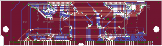
I've done a ton of manual tweaks. I'm not done yet, but I've moved many traces around to allow more of the SIMM to be covered by the ground copper pours on the top and bottom:
There are some great YouTube videos about fine-pitch soldering. You do not and should not have to solder pins individually, except for soldering the corners at first to keep the chip in place. You will soon see that this is WAAAAAY easier than when you soldered PLCC sockets onto the previous revision.
What type of soldering iron do you have? This is the one that I bought, and it works very well for this:
http://www.amazon.com/Weller-WES51-Analog-Soldering-Station/dp/B000BRC2XU
I set it to 75° or so for this sort of thing.
Removing the TSOPs is easy too. You can heat everything up with a pain peeler gun and give it a tap to knock the chips off, or you can use something called ChipQuik. (free samples available!)
What type of soldering iron do you have? This is the one that I bought, and it works very well for this:
http://www.amazon.com/Weller-WES51-Analog-Soldering-Station/dp/B000BRC2XU
I set it to 75° or so for this sort of thing.
Removing the TSOPs is easy too. You can heat everything up with a pain peeler gun and give it a tap to knock the chips off, or you can use something called ChipQuik. (free samples available!)
Yeah -- that's how I solder the AT90USB646 on the programmer board too. Soldering these new chips will basically be the same task except with a finer pitch so I have to be more exact with placement and bridges across pins are more likely to happen.
I have a Hakko FX-888, looks like it has very similar capabilities for temperature settings. I also have some ChipQuik, it's amazing (but expensive)!
I have a Hakko FX-888, looks like it has very similar capabilities for temperature settings. I also have some ChipQuik, it's amazing (but expensive)!
For chips like those, I just run a bead of solder down each row of pins and make sure the whole bead and every pin gets hot enough. Using extra flux helps. Then come back through afterwards with desolder braid and remove any excess. It seems to work surprisingly well for fine pitch soldering.
Agreed--in fact, I'd say flux is the key that makes it all work. I guess the solder has some flux built in, but putting some liquid flux around the pins before soldering seems to help immensely.
Here's my work tonight on the PCB:
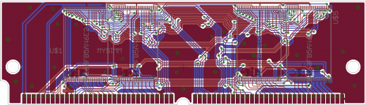
It may look like the copper areas have shrunk, but that's because I increased the isolation for them to 16 mils. Before I increased the isolation, I had actually added extra copper. I'm getting pretty close to having something ready to order
It may look like the copper areas have shrunk, but that's because I increased the isolation for them to 16 mils. Before I increased the isolation, I had actually added extra copper. I'm getting pretty close to having something ready to order
Ooh, looking good... I want to (in annoying commercial voice-over): "Collect all three! Order now!" :b&w:
Haha, that's right! Well, I hope this SIMM works well enough to allow you to collect all three!
I think I'm done laying it out.
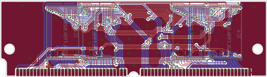
And of course here are the 3D renderings to see what it will look like:
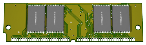
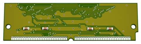
The more I look at the datasheet for the chip, the more I'm pretty sure this is going to work. The chip can do 16- or 8-bit data mode. I force it into 8-bit mode by connecting the byte/word mode selection pin to ground. In this mode, the D15 pin on the chip becomes a byte select pin (high or low byte), essentially becoming the lowest address line.
To unlock the existing 2 MB chips, you write an unlock sequence: $AA to $555555... (filling up all of the address lines with that pattern), then $55 to $AAAAAA... (filling up the address lines with that pattern). Then there's a command set for other stuff.
To unlock these new chips, you write this sequence instead: $AA to $AAAAAA... and $55 to $555555... it's the exact same commands, but the addresses are reversed. I *believe* this is due to the extra byte select pin and my software will actually treat it correctly because the pins starting at A0 do match that pattern, but I don't know for sure. If it doesn't match, it'll be a simple patch to the programmer board's firmware to fix the command patterns for the bigger SIMM.
I think I'm done laying it out.
And of course here are the 3D renderings to see what it will look like:
The more I look at the datasheet for the chip, the more I'm pretty sure this is going to work. The chip can do 16- or 8-bit data mode. I force it into 8-bit mode by connecting the byte/word mode selection pin to ground. In this mode, the D15 pin on the chip becomes a byte select pin (high or low byte), essentially becoming the lowest address line.
To unlock the existing 2 MB chips, you write an unlock sequence: $AA to $555555... (filling up all of the address lines with that pattern), then $55 to $AAAAAA... (filling up the address lines with that pattern). Then there's a command set for other stuff.
To unlock these new chips, you write this sequence instead: $AA to $AAAAAA... and $55 to $555555... it's the exact same commands, but the addresses are reversed. I *believe* this is due to the extra byte select pin and my software will actually treat it correctly because the pins starting at A0 do match that pattern, but I don't know for sure. If it doesn't match, it'll be a simple patch to the programmer board's firmware to fix the command patterns for the bigger SIMM.
ARRRR!!!!! I'll be wanting one to complete me SIMM booty, matey.
I spy lots of room for the Pirates of SIMM Slottage logo, if not the LED(s) on one side, me bucko! [}] ]'>
I spy lots of room for the Pirates of SIMM Slottage logo, if not the LED(s) on one side, me bucko! [}
] ]'>
I'm definitely putting the logo on (arrrrrr!), but I think I'll skip the LEDs this time for simplicity.
How about just one LED and an eye patch? :?:
Now if someone figures out how to convince me IIsi it be somethin' else, we can Rocketize the little snark! [}] ]'>
Now if someone figures out how to convince me IIsi it be somethin' else, we can Rocketize the little snark! [}
] ]'>
I just don't feel good about the LED right now. I want to make sure the board works without anything extra. If it works OK, then in the second batch I might think about LEDs and stuff like that. I guess it's kind of the same way I did it last time.
But I did add the Jolly Roger to the silkscreen
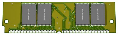
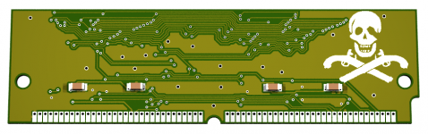
But I did add the Jolly Roger to the silkscreen
ARRRR!!!!!!!!!!!!!! p32, me matey!
Woooooohoooo! This thread is just crazy.
I just sent off gerber files to Seeed Studio for this new board. I cleaned a few more traces at the bottom, and I'm ready to go now. Can't wait to put one together and try it out!
This is also the first SIMM I have done with EAGLE rather than FreePCB, so it's quite a major change. Hopefully it works out OK. The generated gerbers look fine to me at first glance!
I just sent off gerber files to Seeed Studio for this new board. I cleaned a few more traces at the bottom, and I'm ready to go now. Can't wait to put one together and try it out!
This is also the first SIMM I have done with EAGLE rather than FreePCB, so it's quite a major change. Hopefully it works out OK. The generated gerbers look fine to me at first glance!
CONGRATS! What color is it going to be? Blue would be nice and then Black if they finally have it available for the final version w/LED.
Got linkage for Eagle, how much is your license for it? Would FreePCB be enough to do a RAM/SIMM Layout?
Got linkage for Eagle, how much is your license for it? Would FreePCB be enough to do a RAM/SIMM Layout?
I'm going with green for now because it's cheaper. As soon as I'm sure it will work we can pick a better color