

Thread
Another IIci ROM hack
After more research I'm pretty sure it will require a firmware update to use the new 8 megabyte SIMM. This PDF is for Spansion devices, but it's all JEDEC standard stuff from what I can tell.
It's because the flash chip always looks at its A0 through A10 pins for the address to enter unlock mode, even in byte mode where there's an extra address pin (A-1) which goes before A0. I correctly have it wired up so A-1 is the lowest address pin (A-1 is wired to what I call A0 on the SIMM programmer side, A0 is wired to what I call A1, and so on...), but because the chip looks at A0 instead of A-1 for the lowest bit for unlock addresses, the unlock addresses have to be shifted over one bit. It kind of sucks because now the firmware will have to know which type of SIMM you're using, but I'm not too concerned about it -- if you pick a capacity bigger than 2 MB in the control software, it'll just automatically switch the firmware over to the other addressing scheme. I'll have to add something in the firmware so the control software can tell the programmer board what type of SIMM it should be talking with, but that will be simple to add to the communication protocol.
Whatever the case is, it should still work fine And the existing programmer board firmware is really easy to update -- the update process is fail-safe.
It's because the flash chip always looks at its A0 through A10 pins for the address to enter unlock mode, even in byte mode where there's an extra address pin (A-1) which goes before A0. I correctly have it wired up so A-1 is the lowest address pin (A-1 is wired to what I call A0 on the SIMM programmer side, A0 is wired to what I call A1, and so on...), but because the chip looks at A0 instead of A-1 for the lowest bit for unlock addresses, the unlock addresses have to be shifted over one bit. It kind of sucks because now the firmware will have to know which type of SIMM you're using, but I'm not too concerned about it -- if you pick a capacity bigger than 2 MB in the control software, it'll just automatically switch the firmware over to the other addressing scheme. I'll have to add something in the firmware so the control software can tell the programmer board what type of SIMM it should be talking with, but that will be simple to add to the communication protocol.
Whatever the case is, it should still work fine
And the existing programmer board firmware is really easy to update -- the update process is fail-safe.
It should be possible to stay backwards compatible with the older SIMMs and not have to keep reflashing the programmer for different SIMM revs. Here are some ideas:
Mod Programmer firmware only:
- Trial and error both unlock methods, and continue on with the one that worked
- Find some other difference that you can detect between the boards / ROM chips
With programmer application involved:
- Make a SIMM rev. selector in the programmer application, and send a message to the programmer board to select the right unlock method
Mod Programmer firmware only:
- Trial and error both unlock methods, and continue on with the one that worked
- Find some other difference that you can detect between the boards / ROM chips
With programmer application involved:
- Make a SIMM rev. selector in the programmer application, and send a message to the programmer board to select the right unlock method
That's exactly what my plan is. I already have to specify the size of the SIMM in the programmer software, so if they select a size bigger than 2 MB, I'll know it's the new SIMM and can tell the firmware to use the new unlock method.
This is sounding really cool. If I buy a new SIMM, would I still be able to do all the cool boot stuff, and have a bootable Disk Tools because of the extra space?
That's the plan! And in your case, it's really necessary because the DayStar card takes up 512 KB of the available ROM space. Without this bigger SIMM you would only have 1 MB of space available for the Disk Tools disk.
I have made all necessary changes to the firmware and control software already...I just have to wait for the PCBs and chips to arrive!
I have made all necessary changes to the firmware and control software already...I just have to wait for the PCBs and chips to arrive!
Could the programmer software have a 1 chip flash mode?
I would vote for blue/black also...LED is not too essential. Interesting to see SeedStudio is charging an even bigger premium for black. :?:
Purple!
*Edit
laaame

*Edit
laaame
And you were worried about the cost of flash, dougg3!
This seems to be a pretty cost insensitive item if people are wanting to pay more for PCB color!
There are a couple ideas that crossed my mind on this, particularly since reading your other thread about the AV ROM.
1) An AV ROM SIMM would be neat, although probably low volume due to needing to solder a new connector on most of our motherboards. I'd be up for it, my Q630 also has pads for a ROM SIMM.
2) With the 8MB SIMM, new possibilities open up, including running newer, larger ROMs. The IIsi ROM was mainly chosen for the current round of hacking because it had space and was 512KB, which left a pretty usable 1.5MB. But with 8MB, it becomes reasonable to run all the way up to a 2MB AV ROM. That's burning a lot of mostly unnecessary space for the II series machines, but might be worthwhile. The remaining 6MB is still pretty usable, and there are lots of benefits. Some of them being: SCSIMgr4.3, and the EDisk driver. The EDisk driver is quite versatile, including the builtin support for a ROM disk *and* being able to find the ROM disk image inside the ROM. The EDisk driver is both the RAM disk driver and the Classic's ROM disk driver. Which pretty much obsoletes most of the work I've done so far (with the exception of the ROM mapping tables, and disabling both the ROM checksum and the memory test), but such is technology. It'd be interesting to see if SCSIMgr4.3 in the AV ROMs helps the Q900's dual SCSI bus limitations (and the Q900 has the SIMM slot, same as the 700).
This seems to be a pretty cost insensitive item if people are wanting to pay more for PCB color!
There are a couple ideas that crossed my mind on this, particularly since reading your other thread about the AV ROM.
1) An AV ROM SIMM would be neat, although probably low volume due to needing to solder a new connector on most of our motherboards. I'd be up for it, my Q630 also has pads for a ROM SIMM.
2) With the 8MB SIMM, new possibilities open up, including running newer, larger ROMs. The IIsi ROM was mainly chosen for the current round of hacking because it had space and was 512KB, which left a pretty usable 1.5MB. But with 8MB, it becomes reasonable to run all the way up to a 2MB AV ROM. That's burning a lot of mostly unnecessary space for the II series machines, but might be worthwhile. The remaining 6MB is still pretty usable, and there are lots of benefits. Some of them being: SCSIMgr4.3, and the EDisk driver. The EDisk driver is quite versatile, including the builtin support for a ROM disk *and* being able to find the ROM disk image inside the ROM. The EDisk driver is both the RAM disk driver and the Classic's ROM disk driver. Which pretty much obsoletes most of the work I've done so far (with the exception of the ROM mapping tables, and disabling both the ROM checksum and the memory test), but such is technology. It'd be interesting to see if SCSIMgr4.3 in the AV ROMs helps the Q900's dual SCSI bus limitations (and the Q900 has the SIMM slot, same as the 700).
for large ROM space, isnt there a possibility of using a small scale micro-FPGA? using such with a serial flash and a RAM IC thats large enough to handle everything?
For example, soon as power hits the SIMM, the FPGA copies/decompresses the SPI flash into the RAM IC and everything runs from the RAM IC in a parallel state, whilst the FPGA is managing the RAS/CAS of the RAM to keep it refreshed. There are open source FPGA code out there for VHDL on controlling all RAM up to DDR3. FPGA would be used as the buffer, a read request comes from the ROM space, so the FPGA fetches it from RAM and puts it on the bus.
For example, soon as power hits the SIMM, the FPGA copies/decompresses the SPI flash into the RAM IC and everything runs from the RAM IC in a parallel state, whilst the FPGA is managing the RAS/CAS of the RAM to keep it refreshed. There are open source FPGA code out there for VHDL on controlling all RAM up to DDR3. FPGA would be used as the buffer, a read request comes from the ROM space, so the FPGA fetches it from RAM and puts it on the bus.
Yes -- I have some of the work done on it already. All the chips are tied together with their control lines, but I can just send the wrong data bytes to the other chips (if present) during the unlock sequence to skip erasing/programming them. The code is there -- I just have to add it to the communication protocol and add capabilities to the control software to activate it.
Yeah...it's weird! But yeah, something like blue or black sounds great to me.
Sorry!Purple!
*Edit
laaame
Haha...well if that's the case, let's find a manufacturer who can do silkscreen in orange or something awesome like that!

Yeah, the lack of soldered sockets is a problem with making ROM SIMMs for other models. I have a ton of 64-pin SIMM sockets thanks to olePigeon, but it's a pain in the butt to add the sockets to the motherboard. For that reason I'm not sure that I really want to create one. Honestly, it's similar enough that I could probably just reuse the existing SIMM PCB and just add a switch or something for "program mode" vs. "in-Mac mode" that sets the chip select line as needed.
I wonder if the Q630's ROM SIMM uses the same pinout? I think I have a Performa 630 here somewhere, I could check it out with a multimeter. Or maybe the dev notes for it say the pinout...I'm too lazy to check now.
The EDisk driver seems like a really interesting idea. Does it work in the same conditions as the things you've had to work around, such as the "only 1 MB of ROM space available in 24-bit addressing" problem?
BTW, I've flashed an AV ROM onto my SIMM and tried to boot my IIci with it -- it doesn't work
But it would be AWESOME if we could figure out why it doesn't work and make it work. That would be great to get everything up and running on the latest 68k Mac ROM.---
Latest update: the chips have arrived. I was expecting Micron chips and got ST chips, but I did some research and I now understand what happened. It looks like what happened is that back in 2008, Intel and ST Microelectronics spun off their flash chips into a new company called Numonyx, which Micron later bought. So these are old chips back from when ST still called them their own.
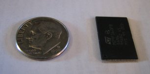
It's so tiny...I can't wait to assemble one of these SIMMs!
Hey i actually have a bunch of ZIF TSOP sockets that fit these, i think they do anyway, not sure of the pincount, i think its TSOP48 I have.
Yeah, it should pretty much have the same behavior. You can't get any more ROM space in 24bit mode since 0x900000 is Slot 9's 24bit address space. But it should bounce between modes like my driver does, so it should still be accessible even when using a 24bit app or whatever. I'm not sure it has the ability to copy the disk image into RAM to have a writeable boot volume though.
The AV ROMs have a different way of setting up ROM space from the IIsi ROM, which may be related to at least one of the reasons why it won't boot. I might try to poke at this a bit.
I actually really like this idea. Big RAM and large SPI flashes are a lot easier to find than big parallel flashes. My main question about this approach is: how can you get the data out of the serial flash and into the RAM before the CPU does its first access to the ROM? The very first access by the CPU is to ROM to grab the reset vector. That's going to be very very early in the boot process, possibly before the FPGA has had a chance to load much data into RAM. Maybe still use a parallel NOR flash for the lower 1 MB or 2 MB of space and then use the FPGA for accesses above that?
Although there is only 8 MB of available address space in the ROM space, you could use the FPGA to create a register somewhere in the 8 MB of address space to control which page is currently active. The lower 2 MB or 4 MB could always be mapped to the ROM, and the rest of the address space could change depending on which page is selected. The disk driver could use the page selection register to create a practically unlimited ROM disk size. Just dreaming here...
Yeah, these are TSOP48 chips. I didn't even realize that ZIF sockets existed for fine-pitch surface mount components like this. Do the sockets solder onto the same pad layout that the chips solder onto?
Well, that's interesting! It would be pretty cool to make it work with Apple's stock RAM/ROM disk driver, I have to admit.
Edit: I just realized after reading the datasheet for the chips I'm using that they aren't available in the SO44 package. Probably because the TSOP48 package uses 46 of the 48 pins (GND is duplicated, so only 45 are really necessary). Either way, 45 and 46 are still larger than 44. That would explain why it's not available in the SO44 package...so I was wrong earlier when I said I knew this chip was available in SO44.
As long as you are using an FPGA, you could have 2 modes of operation. "loading ROM" mode and "ready" mode.
In "loading ROM" mode, you can hard-code this sort of functionality:
Reset vector:
location 0x0000 0000
At Location 0x0000 0000:
Load reset vector with location 0xXXXX XXXX (default with 0x0000 0000)
Branch to reset vector
The Mac would sit and spin in this mode, changing addresses back and forth so you have something for synchronization to avoid a race condition. When the FPGA is ready and the address changes to 0x0000 0000, swap in the actual reset vector from actual ROM. When the address changes to the reset vector, swap in the ENTIRE actual ROM for ready mode.
I don't think it's out of the question to add clips to the Mac as an optional feature. This would allow us to run additional address lines to the ROM SIMM by clipping them onto the processor's pins or some other convenient spot. Each additional line doubles the maximum ROM capacity. Even supplying thru-holes for a small pin header on an edge of the ROM SIMM would allow people to make these connections on their own for increased capacity. There were certainly commercial Mac upgrades that used clips and it think it would appeal to some of us geeks to know that at least the capability exists.
Ah, that makes sense! Just force it into an endless loop of nothing until the RAM has been completely loaded from the SPI flash and then unlock it. I get it, nice idea!
The clips are an interesting idea. I think it would work as long as we guaranteed that $40800000 (32-bit) and $800000 (24-bit) pointed to the actual ROM because that's what the Mac OS uses for its base address. With the other address clips in place we would be free to use $40000000 to $407FFFFF and $40880000 to $4FFFFFFF for whatever we wanted...that's a lot of space available if the address lines are easily clippable!
The clips are an interesting idea. I think it would work as long as we guaranteed that $40800000 (32-bit) and $800000 (24-bit) pointed to the actual ROM because that's what the Mac OS uses for its base address. With the other address clips in place we would be free to use $40000000 to $407FFFFF and $40880000 to $4FFFFFFF for whatever we wanted...that's a lot of space available if the address lines are easily clippable!
With this theoretical FPGA / RAM module on a ROM SIMM, would it be feasible to then make a volatile read/write ROM disk? How about Non-volatile? I'm not aware of how the 68k does a write operation to memory or if that signal is available in the ROM SIMM slot.
I don't know how the 68k does it either, but a write signal is not available in the ROM SIMM. We'd probably need to find it somewhere else. Also, I don't know for sure, but the MMU might have to be set up to allow writes to that region.
I think it would be feasible at that point to make a volatile ROM disk (although bbraun has already done this by copying the ROM disk contents into RAM and doing a RAM disk). I'm not sure about non-volatile...if each write could wait for the SPI flash to finish its corresponding write, I think it could be done.
With all that said, I don't know the first thing about FPGAs other than basically how to control an LED with a push button in VHDL and I also don't know how fancy of an FPGA we would need to meet the ROM timing requirements...
I think it would be feasible at that point to make a volatile ROM disk (although bbraun has already done this by copying the ROM disk contents into RAM and doing a RAM disk). I'm not sure about non-volatile...if each write could wait for the SPI flash to finish its corresponding write, I think it could be done.
With all that said, I don't know the first thing about FPGAs other than basically how to control an LED with a push button in VHDL and I also don't know how fancy of an FPGA we would need to meet the ROM timing requirements...
For non-volatile, there is probably no way to directly write to the Flash in real time, so it would need to be buffered or double buffered. If we can supply twice as much RAM on this SIMM as ROM, then that would give us space for a double buffer. When the SIMM first powers on, it would need to make two copies of ROM into RAM. One of these copies would be the "working" copy, the version that the Mac uses directly. The other copy would be a representation of the flash contents.
That allows us to add a function to the FPGA that constantly cycles through the RAM and compares the working copy to the buffer. When it finds a difference, it would then update the Flash with a write operation. This method uses the minimum number of write cycles to the Flash which will prolong its life.
A different option, the single buffer, uses less RAM but uses a lot more write cycles. You could set a flag on any write operation, then based on this flag, handle it by turning the flag off and writing all Flash from the information stored in the SIMM's RAM. If the flag is set again during the update, it will do another update again at the end of the current update. If the flag is set 10 minutes later, then all of the time in between will be spent not updating to preserve write cycles.
That allows us to add a function to the FPGA that constantly cycles through the RAM and compares the working copy to the buffer. When it finds a difference, it would then update the Flash with a write operation. This method uses the minimum number of write cycles to the Flash which will prolong its life.
A different option, the single buffer, uses less RAM but uses a lot more write cycles. You could set a flag on any write operation, then based on this flag, handle it by turning the flag off and writing all Flash from the information stored in the SIMM's RAM. If the flag is set again during the update, it will do another update again at the end of the current update. If the flag is set 10 minutes later, then all of the time in between will be spent not updating to preserve write cycles.
There are of course intermediate options to improve the single buffer method as well, for example, having a multitude of flags for discrete chunks of memory, then updating just the chunks that have been flagged.
I'm brainstorming here - not necessarily is any of this reasonable or within scope for these hobbiest gizmos, but it's at least fun to think about and useful when making more realistic ideas.
I'm brainstorming here - not necessarily is any of this reasonable or within scope for these hobbiest gizmos, but it's at least fun to think about and useful when making more realistic ideas.
Ah, yeah...some kind of buffering would probably be needed. I forgot that it's not just a byte-per-byte write and erase thing when you're dealing with flash.
What about using an SD card rather than an SPI flash? I *think* an SD card would be easier because it will handle the wear-leveling internally and just present itself as a block device that can be read/written in 512-byte chunks. I don't know if that's useful at all, but I'm guessing the convenience of being able to pull the card out and plug it into the computer to be reflashed would be useful.
I know that write performance isn't the best with SD cards, but it's just a thought...
What about using an SD card rather than an SPI flash? I *think* an SD card would be easier because it will handle the wear-leveling internally and just present itself as a block device that can be read/written in 512-byte chunks. I don't know if that's useful at all, but I'm guessing the convenience of being able to pull the card out and plug it into the computer to be reflashed would be useful.
I know that write performance isn't the best with SD cards, but it's just a thought...
Yes the TSOP48 sockets i have sit right on the footprint the chip would go, its designed that way on purpose so you can pull the TSOP off a board, and put a socket in place so you can debug without in-circuit flashing ability.
I picked a few of these up and never used them.
Also, as far as the FPGA goes, does the RESET signal come to the ROM slot? i cant remember. if so, you can hold the bus into RESET until its finished loading. then free the bus. Dennis' method would work just as fine as well. But requires additional logic blocks in the FPGA to keep the bus in a loop. then once its complete, use a mux or something in VHDL to switch over. Nice thing about having this type of a setup, you can hot-flash the SPI inside the mac while its running with an application, as long as you have FPGA blocks to support it, without touching the RAM contents so the "ROM" dont change on the mac while your flashing it. Then reboot once done, if the RESET signal comes to the SIMM the FPGA can pick up this signal and start its entire SPI to RAM loading process over again. Regardless, i think you need to watch the RESET condition as a signal to start the process.
Either watch this pin, or decode the reset vector on the bus, if the FPGA detects it, reload SPI to RAM and hang RESET until complete. Since we are doing some real simple tasks, i think a micro FPGA would work just fine, and would fit on the SIMM. The only drawback is finding an FPGA that runs on 5V only. most are 3.3v, 1.8v, or a combination of voltages. one for IO, one for Core, etc... in which case youll need small SOT-89 V-Regs on the board to handle this, some 3.3V FPGAs are 5V tolerant so make sure you look at that aspect as well, it could be a trap if no attention is paid. ;-)
there are some open-source softcores too so if you wanted to put some "brain" on the SIMM for advanced operations outside of logic, in theory, you could such as the flashing algo for SPI would have to be run on a softcore unless you know of a way to code it specifically as logic in VHDL. If you ran out of on-chip storage, you could always compress the code that would run on the softcore and expand it at the "end" block of the RAM chip and boot the code from there for the softcore to SPI flash, etc... many many many options.
Hell if the architecture supports cache RAM, you could add an FPGA block to address out some RAM space for caching. speed up the machine.
Sorry for the rambling, its just some info. I am FPGA dumb, but i do know how they work to an extent, and learning as I go.
I picked a few of these up and never used them.
Also, as far as the FPGA goes, does the RESET signal come to the ROM slot? i cant remember. if so, you can hold the bus into RESET until its finished loading. then free the bus. Dennis' method would work just as fine as well. But requires additional logic blocks in the FPGA to keep the bus in a loop. then once its complete, use a mux or something in VHDL to switch over. Nice thing about having this type of a setup, you can hot-flash the SPI inside the mac while its running with an application, as long as you have FPGA blocks to support it, without touching the RAM contents so the "ROM" dont change on the mac while your flashing it. Then reboot once done, if the RESET signal comes to the SIMM the FPGA can pick up this signal and start its entire SPI to RAM loading process over again. Regardless, i think you need to watch the RESET condition as a signal to start the process.
Either watch this pin, or decode the reset vector on the bus, if the FPGA detects it, reload SPI to RAM and hang RESET until complete. Since we are doing some real simple tasks, i think a micro FPGA would work just fine, and would fit on the SIMM. The only drawback is finding an FPGA that runs on 5V only. most are 3.3v, 1.8v, or a combination of voltages. one for IO, one for Core, etc... in which case youll need small SOT-89 V-Regs on the board to handle this, some 3.3V FPGAs are 5V tolerant so make sure you look at that aspect as well, it could be a trap if no attention is paid. ;-)
there are some open-source softcores too so if you wanted to put some "brain" on the SIMM for advanced operations outside of logic, in theory, you could such as the flashing algo for SPI would have to be run on a softcore unless you know of a way to code it specifically as logic in VHDL. If you ran out of on-chip storage, you could always compress the code that would run on the softcore and expand it at the "end" block of the RAM chip and boot the code from there for the softcore to SPI flash, etc... many many many options.
Hell if the architecture supports cache RAM, you could add an FPGA block to address out some RAM space for caching. speed up the machine.
Sorry for the rambling, its just some info. I am FPGA dumb, but i do know how they work to an extent, and learning as I go.
This gets me thinking about microcontroller vs. FPGA because talking in serial is good for microcontrollers and talking right away in parallel is good for FPGAs. I'm starting to wonder if we could get by with just a microcontroller. FPGAs are fairly complicated to program in my experience.
I haven't seen it done much in the hobby world, but maybe USB could be an option? I've heard that hosting USB has a lot of overhead. USB opens the door to flash drives, hard drives, and USB-to-memory card converters. I'm thinking that you get non-SPI, high-speed access to SD cards that way. Using a microcontroller also adds the possibility of filesystem support, so you can store the ROM data in a file on the USB storage device, allowing you to mount the USB device on a computer and copy / modify the file. A ROM burner or special application would no longer be necessary.
I haven't seen it done much in the hobby world, but maybe USB could be an option? I've heard that hosting USB has a lot of overhead. USB opens the door to flash drives, hard drives, and USB-to-memory card converters. I'm thinking that you get non-SPI, high-speed access to SD cards that way. Using a microcontroller also adds the possibility of filesystem support, so you can store the ROM data in a file on the USB storage device, allowing you to mount the USB device on a computer and copy / modify the file. A ROM burner or special application would no longer be necessary.
the thing is, the microcontroller would have to be very very fast, as you would need a bit of headroom between bus cycles. and then you need DRAM controller/timing code for DDR chips or whatever RAM you use. Thats why i think an FPGA would be better suited but use a softcore for the MCU part of the tasks.
an MCU alone is sufficient if your loading from a storage medium or etc to Shadow RAM for the ROM. But the bus handling of the RAM is where things get tricky. You need headroom between each bus cycle so you can do things such as refresh the RAM, fetch the data, etc.. So when the bus cycle comes the data is ready for it, and it has to be fast between each phase. So when the address phase comes, the CPU can quickly refresh and fetch the data from the RAM to be put onto the bus. It could be doable, but your not doing it with your standard 8-bit micro. you would almost need a propeller which has multi-cores, or maybe an ARM based MCU with fast I/O.
You basically would have to calculate the time period that would occur between each complete bus cycle at its fastest possible point it ever could, and each phase within the bus cycle, that way you can pick up a suitable microcontroller and speed that would be able to get quite a few machine cycles completed within that period. Then youll be ok.
So if for example the MCU can execute at least 10 to 12 instructions between a cycle period, maybe 4 instructions between a phase period then if you keep things fast and tight, its doable to fetch the data in time.
an MCU alone is sufficient if your loading from a storage medium or etc to Shadow RAM for the ROM. But the bus handling of the RAM is where things get tricky. You need headroom between each bus cycle so you can do things such as refresh the RAM, fetch the data, etc.. So when the bus cycle comes the data is ready for it, and it has to be fast between each phase. So when the address phase comes, the CPU can quickly refresh and fetch the data from the RAM to be put onto the bus. It could be doable, but your not doing it with your standard 8-bit micro. you would almost need a propeller which has multi-cores, or maybe an ARM based MCU with fast I/O.
You basically would have to calculate the time period that would occur between each complete bus cycle at its fastest possible point it ever could, and each phase within the bus cycle, that way you can pick up a suitable microcontroller and speed that would be able to get quite a few machine cycles completed within that period. Then youll be ok.
So if for example the MCU can execute at least 10 to 12 instructions between a cycle period, maybe 4 instructions between a phase period then if you keep things fast and tight, its doable to fetch the data in time.
I'm not totally straight on how RAM sticks work on a signal level. I understand that something has to go through and refresh the contents of RAM constantly. Is this process within the realm of a microcontroller's ability? Also, for this RAMmish ROM SIMM, can address and data connections be made directly to the RAM so that the Mac talks only to the RAM and not "through" the microcontroller / FPGA? Or does there have to be logic between the RAM stick and Mac's busses?
If the Mac can interface directly with the RAM, and if the ROM data is in the RAM, then it should be able to read it right away regardless of how slow the microcontroller is?
If the Mac can interface directly with the RAM, and if the ROM data is in the RAM, then it should be able to read it right away regardless of how slow the microcontroller is?
I dont know the full detail on how RAS/CAS timing and refresh cycles work, but i do know that on an ATmel AVR series microcontroller, it barely has enough speed to run and refresh 30pin SIMM type DRAM. its been done, but its not a good candidate.
There is open source VHDL code out there for DDR1 2, and 3 RAM chips for reading/writing/controlling those ICs maybe looking at that could turn up some results on how they work? I guess the RAS/CAS/CL numbers you see on computer RAM sticks is the requirements to keep the data inside valid...
But as far as being able to bus directly to the RAM, i dont know. I dont think so because the FPGA or DRAM controller has to mux itself in at some point to refresh the RAM. If you look at the SE/30 schematics there is a PAL chip and several muxes that do just this.
the memory/system bus via the PALs are timed in such a way that when a read or write operation happens to the SE/30 RAM, it always occurs in between the refresh cycle, it does not occur right at the same time the RAM is being refreshed, so the bus doesnt get halted or some type of GPF occurs. I have studied that circuit until my eyes went crosseyed for troubleshooting reasons, and thats what I have gathered.
There is open source VHDL code out there for DDR1 2, and 3 RAM chips for reading/writing/controlling those ICs maybe looking at that could turn up some results on how they work? I guess the RAS/CAS/CL numbers you see on computer RAM sticks is the requirements to keep the data inside valid...
But as far as being able to bus directly to the RAM, i dont know. I dont think so because the FPGA or DRAM controller has to mux itself in at some point to refresh the RAM. If you look at the SE/30 schematics there is a PAL chip and several muxes that do just this.
the memory/system bus via the PALs are timed in such a way that when a read or write operation happens to the SE/30 RAM, it always occurs in between the refresh cycle, it does not occur right at the same time the RAM is being refreshed, so the bus doesnt get halted or some type of GPF occurs. I have studied that circuit until my eyes went crosseyed for troubleshooting reasons, and thats what I have gathered.
This is a good document on DRAM:
http://www.ece.cmu.edu/~ece548/localcpy/dramop.pdf
its pretty much the rough concept of it and how its supposed to work.
http://www.ece.cmu.edu/~ece548/localcpy/dramop.pdf
its pretty much the rough concept of it and how its supposed to work.
Here is another more detailed, and newer document that goes into SDRAM and DDR:
http://smithsonianchips.si.edu/ice/cd/MEMORY97/SEC07.PDF
with SDRAM you can do concurrent operations, such as refresh AND read at the same time, So no collisions.
But you still need some logic. Why? because DRAM is broken into rows and columns so you would need an address decoder at the minimum to turn an address into a row/column fetch, in sync with a counter that keeps refresh as well. This way the fetch is valid and the RAM is still being refreshed. The returned data can be placed onto the bus when the bus requests the OE. This is simple mux/counter/decoder logic in a FPGA, or code in an MCU, with MCUs though you have to keep an accurate sync on the bus or you can get race/lag conditions. lol. I am not sure of the window on ROM as in how fast the data needs to be on the bus at the time of an address/fetch. RAM is like 70 to 140ns, ROM i dont know. but you have to be within that window or it may not boot so if the MCU takes too long to fetch the data out of RAM with a given address, your up shit creek without a paddle.
http://smithsonianchips.si.edu/ice/cd/MEMORY97/SEC07.PDF
with SDRAM you can do concurrent operations, such as refresh AND read at the same time, So no collisions.
But you still need some logic. Why? because DRAM is broken into rows and columns so you would need an address decoder at the minimum to turn an address into a row/column fetch, in sync with a counter that keeps refresh as well. This way the fetch is valid and the RAM is still being refreshed. The returned data can be placed onto the bus when the bus requests the OE. This is simple mux/counter/decoder logic in a FPGA, or code in an MCU, with MCUs though you have to keep an accurate sync on the bus or you can get race/lag conditions. lol. I am not sure of the window on ROM as in how fast the data needs to be on the bus at the time of an address/fetch. RAM is like 70 to 140ns, ROM i dont know. but you have to be within that window or it may not boot so if the MCU takes too long to fetch the data out of RAM with a given address, your up shit creek without a paddle.
Basically in a nutshell, your using the FPGA to do one main purpose. To convert the DDR Dram into PSRAM. which basically looks like regular SRAM on the bus. as SRAM and ROM are accessed identically, only difference being SRAM is temporary and ROM is well, permenent aside bitrot.
You actually might be able to buy PSRAM outright with the refresh controller actually built into the IC. If thats the case, you can use it as SRAM and dont need any FPGA or associated circuitry. Just an MCU to copy SPI flash or other source to the RAM before boot.
P.S. Matter of fact, here is a document to do just that...
http://www.fujitsu.com/downloads/MICRO/fma/pdf/psram.pdf
life just got ALOT more simple. You will still need at least minimally an MCU and mux to switch it off the bus during a write. Also PSRAM is still in active development because its used for low-power/mobile market. Also do you want to upgrade the memory in your mac portable? yea.. welll.... thats a possibility too.
128Megabit (8Megabyte) PSRAM chips are cheap too, between 6 to 11 dollars depending on who you go with. They are BGA mount however, but they are MBGA48s which are simple to mount with a heatgun and a hotplate/pancake griddle. I used to mount EBGA64s this way.
Datasheet:
http://download.micron.com/pdf/datasheets/psram/128mb_burst_cr1_5_p26z.pdf
That chip is perfect. 16bit I/0, 22bit addressing. 128Megabit chip, which is 8megabytes or 4megawords. being that its a 16bit output, you would see 2 bytes at a time. These chips are also about $13 from digikey. probably cheaper than 4 flash TSOPs, but you still have to factor in the logic for the processor required to put the information INTO the RAM ;-)
You actually might be able to buy PSRAM outright with the refresh controller actually built into the IC. If thats the case, you can use it as SRAM and dont need any FPGA or associated circuitry. Just an MCU to copy SPI flash or other source to the RAM before boot.
P.S. Matter of fact, here is a document to do just that...
http://www.fujitsu.com/downloads/MICRO/fma/pdf/psram.pdf
life just got ALOT more simple. You will still need at least minimally an MCU and mux to switch it off the bus during a write. Also PSRAM is still in active development because its used for low-power/mobile market. Also do you want to upgrade the memory in your mac portable? yea.. welll.... thats a possibility too.
128Megabit (8Megabyte) PSRAM chips are cheap too, between 6 to 11 dollars depending on who you go with. They are BGA mount however, but they are MBGA48s which are simple to mount with a heatgun and a hotplate/pancake griddle. I used to mount EBGA64s this way.
Datasheet:
http://download.micron.com/pdf/datasheets/psram/128mb_burst_cr1_5_p26z.pdf
That chip is perfect. 16bit I/0, 22bit addressing. 128Megabit chip, which is 8megabytes or 4megawords. being that its a 16bit output, you would see 2 bytes at a time. These chips are also about $13 from digikey. probably cheaper than 4 flash TSOPs, but you still have to factor in the logic for the processor required to put the information INTO the RAM ;-)
p. 33 8-o
This discussion got too far above my head for a bit, so I've ignored it for a while. Looka like I'd better get current on this while I have a chance!
Meanwhile, back to simple problems. DQ & Company, when you test all these different ROM/Mac combos, the Gestalt IDs remain the same when a new combo works, correct? Could the Gestalt Id's five bits of information be simple component(s) on the MoBo that are addressed over I2C before the CPU queries the ROM addresses?
I need to tell my IIsi that it's something like a Quadra 700. That way the Radius Rocket,RocketWare Installer a/o RocketWare itself, will think it's compatible with the Stealth IIsi.
Whatcha think guys?
This discussion got too far above my head for a bit, so I've ignored it for a while. Looka like I'd better get current on this while I have a chance!
Meanwhile, back to simple problems. DQ & Company, when you test all these different ROM/Mac combos, the Gestalt IDs remain the same when a new combo works, correct? Could the Gestalt Id's five bits of information be simple component(s) on the MoBo that are addressed over I2C before the CPU queries the ROM addresses?
I need to tell my IIsi that it's something like a Quadra 700. That way the Radius Rocket,RocketWare Installer a/o RocketWare itself, will think it's compatible with the Stealth IIsi.
Whatcha think guys?
The gestaltMachineType values are based on what the ROM detects from the hardware. AFAIK, this value is an ultra-boiled down version of what the GetHardwareInfo/GetExtHardwareInfo ROM routines generate. Those routines are somewhat complicated (I just went over their disassembly yesterday) since there's all kinds of different ways various boards identify themselves, but for the machines covered by the Guide to the Macintosh Family Hardware, it is mostly determined by VIA values as documented in Chapter 4.
For other machines, the MESS guys have some information in their Technical Notes
But, as has been covered before there are many ways to try to check what machine you're on. "Wish I Were" changes the gestalt value (which is easy to do, like I did for the system version gestalt, so I doubt they're looking at just the gestalt value.
All that aside, the first thing you need to do is determine what they're checking. My suspicion is, in the end it'd just be better to patch RocketWare.
For other machines, the MESS guys have some information in their Technical Notes
But, as has been covered before there are many ways to try to check what machine you're on. "Wish I Were" changes the gestalt value (which is easy to do, like I did for the system version gestalt, so I doubt they're looking at just the gestalt value.
All that aside, the first thing you need to do is determine what they're checking. My suspicion is, in the end it'd just be better to patch RocketWare.