

Thread
Another IIci ROM hack
Was it discussed already about putting a CF card reader on a ROM SIMM? Or is 8MBs the biggest size? Would be cool to stick a 256MB card in there and just go diskless. 
8 MB is the limit of the ROM slot, after that you have to start adding clips for more address lines, if it can work that way. Each clip would double the max ROM if the memory controller allows this.
Max ROM SIMM = 8 MB * 2 ^ (# of clips)
We also talked about using some sort of large flash drive/CF/SD card, but this presents a problem because they are serial and the Mac expects parallel ROM. It would be difficult to convert serial to parallel fast enough for that to work.
Max ROM SIMM = 8 MB * 2 ^ (# of clips)
We also talked about using some sort of large flash drive/CF/SD card, but this presents a problem because they are serial and the Mac expects parallel ROM. It would be difficult to convert serial to parallel fast enough for that to work.
I've thought about it, but there are a couple of problems:
The ROM SIMM slot pinout only provides for 8 MB of space, so you'd have to do extra hardware hacks to get more address lines. Might be better to do a PDS type card instead because of that.
You have to get the data off the CF card and onto the data bus fast enough. It's going to require some kind of controller/FPGA/whatever in between to read from the CF card and stick it on the bus fast enough, or use RAM or . I think on the past couple of pages people were discussing ways to make it happen -- but that 8 MB limit is still a problem.
I was thinking if a ROM disk was the main reason we wanted to use the extra space, a ROM disk driver could change between different 7.5-MB pages by writing to a register (which would be handled by the FPGA) to pick the selected page. This is how 16-bit microcontrollers handle addressing more than 64 KB of space, for example. So you'd still only need the 8 MB of address lines in that case. It would be pretty complicated to get working though. I believe this is also how Nintendo games were able to address larger amounts of program space as well.
Edit: What Dennis Nedry said.
Edit2: I forgot the "write" line doesn't come out to the SIMM. It would have to be something like what bbraun described. Maybe a read from a specific address followed by another read to select a bank or command or something?
The ROM SIMM slot pinout only provides for 8 MB of space, so you'd have to do extra hardware hacks to get more address lines. Might be better to do a PDS type card instead because of that.
You have to get the data off the CF card and onto the data bus fast enough. It's going to require some kind of controller/FPGA/whatever in between to read from the CF card and stick it on the bus fast enough, or use RAM or . I think on the past couple of pages people were discussing ways to make it happen -- but that 8 MB limit is still a problem.
I was thinking if a ROM disk was the main reason we wanted to use the extra space, a ROM disk driver could change between different 7.5-MB pages by writing to a register (which would be handled by the FPGA) to pick the selected page. This is how 16-bit microcontrollers handle addressing more than 64 KB of space, for example. So you'd still only need the 8 MB of address lines in that case. It would be pretty complicated to get working though. I believe this is also how Nintendo games were able to address larger amounts of program space as well.
Edit: What Dennis Nedry said.
Edit2: I forgot the "write" line doesn't come out to the SIMM. It would have to be something like what bbraun described. Maybe a read from a specific address followed by another read to select a bank or command or something?
One could still use the ROM slot for more storage though. Put some registers somewhere in the 8MB addressable space, and a device driver (we're already using one as it stands) could access an arbitrarily large backing store through polled access of those registers. It'd work more efficiently through an interface that had an interrupt line, but still seems doable just through the ROM slot. And of course it doesn't necessarily even need to be accessing storage, it could be accessing a USB device, or network, or even another processor.
Device drivers sounds cool. Is it possible to put extensions on the ROM SIMM? Would be cool if SCSI, Zip, Jaz, or MO drivers were loaded on ROM so you don't need to have any extensions on the machine. Someone mentioned putting SCSI Manager on the ROM?
As far as what can be put in the ROM, in theory anything can. It's only software, right? 
When I typically use the term 'device driver' on Mac OS, I'm referring to resources of type 'DRVR'. Those conform to a specific interface and can be manipulated by system API. The only thing that's required for those to work in the ROM is they be added to the resource section of the ROM, and some code somewhere needs to call _Open with the device driver's name (in theory). My ROM Disk driver does this by replacing the unused .netBOOT driver in the resource section of the ROM, and the ROM already has code to call _Open on that driver, so all of that happens for "free".
There's only so many unused entries in the ROM resource section to be repurposed. Eventually, it may be necessary to move the entire resource section past the end of the regular ROM so it has room to grow. The resources within the ROM should be self referential (as in, not have relative offsets to other parts of the ROM outside themselves), so moving the entire thing is probably going to be safer than trying to grow it in place and move code that comes after it, which is definitely being referenced through relative offsets from elsewhere in the ROM.
But, resources of type 'DRVR' are only a specific set. Extensions are things that have resources of type 'INIT', which is a code resource that gets run at specific times during OS boot. That all gets a little more tricky, especially since the 'INIT' code typically loads other resources within the extension file, like icons to display at boot time, or just to load and run 'DRVR' drivers. Those might be evaluated on a case by case basis, I think.
Anyway, the gist of the whole thing is: maybe?
Specific instances can be investigated on a case by case basis, I think.
When I typically use the term 'device driver' on Mac OS, I'm referring to resources of type 'DRVR'. Those conform to a specific interface and can be manipulated by system API. The only thing that's required for those to work in the ROM is they be added to the resource section of the ROM, and some code somewhere needs to call _Open with the device driver's name (in theory). My ROM Disk driver does this by replacing the unused .netBOOT driver in the resource section of the ROM, and the ROM already has code to call _Open on that driver, so all of that happens for "free".
There's only so many unused entries in the ROM resource section to be repurposed. Eventually, it may be necessary to move the entire resource section past the end of the regular ROM so it has room to grow. The resources within the ROM should be self referential (as in, not have relative offsets to other parts of the ROM outside themselves), so moving the entire thing is probably going to be safer than trying to grow it in place and move code that comes after it, which is definitely being referenced through relative offsets from elsewhere in the ROM.
But, resources of type 'DRVR' are only a specific set. Extensions are things that have resources of type 'INIT', which is a code resource that gets run at specific times during OS boot. That all gets a little more tricky, especially since the 'INIT' code typically loads other resources within the extension file, like icons to display at boot time, or just to load and run 'DRVR' drivers. Those might be evaluated on a case by case basis, I think.
Anyway, the gist of the whole thing is: maybe?
Specific instances can be investigated on a case by case basis, I think.
Just brainstorming here after pondering Dennis Nedry and bbraun's replies...
How about leaving the first 4 MB of ROM SIMM space as regular ROM? It is still connected directly to a flash chip, so no problems booting at all -- it's already all parallelized and ready to go right off the bat. Connect the SIMM /OE pin and the appropriate SIMM address pin to an AND gate's input, and connect the AND gate's output to the ROM chips' /OE pins -- I think that would be sufficient to disable the ROM chips' outputs in the second half of the ROM SIMM space. Maybe not an AND gate, but whatever gate is appropriate (too lazy to think about it right now).
Then, drivers patched into that ROM space read from various locations in the second 4 MB of ROM SIMM space to do things. To "write" to it, you could read from a certain address inside that space, followed by four consecutive reads from a 256-byte space to specify the address, and another four consecutive reads to specify the data. Example:
I want to write $12345678 to $ABCDEF00 (which might be a register I've created in the FPGA for something--a memory page selection register or an SD card controller register or whatever). The "begin write" register is at $40C00000, and the "write address/data" registers are from $40C00100 to $40C001FF.
So I start by reading from $40C00000. The FPGA notices this and starts listening for reads from the "write address/data registers" registers. Next, I read from $40C001AB, $40C001CD, $40C001EF, and $40C00100, in that order. Now the FPGA knows I want to write to the address $ABCDEF00, and waits for 4 more read cycles to figure out the data to write. So I read from $40C00112, $40C00134, $40C00156, and $40C00178. Now the FPGA knows both the address and the data I wanted to write, so it does the write. Finally, there could be some kind of a status register to poll to determine completion of the write (if necessary).
Obviously, this is slow because it takes 9 read cycles to do a single "write cycle". Is that a big problem? For faster performance, I could reserve a 64K space rather than a 256-byte space and do two bytes at a time. That would only require 5 read cycles. I could probably cut it down to 4 read cycles by combining the first $40C00000 read cycle with the first "write address" read cycle, perhaps in a new 64K space so I still have sync information to know when a read begins.
Using this technique, I'm pretty sure we could do *anything* we want with the ROM SIMM slot, no extra hardware mods required. Map a huge CF card, SD card, or any other peripheral like bbraun pointed out.
Of course, routing the board would be tricky, but it could probably be done...may need 4 layers to fit the FPGA/sockets/etc. on the board though.
Wow...I think my mind is about to explode now.
How about leaving the first 4 MB of ROM SIMM space as regular ROM? It is still connected directly to a flash chip, so no problems booting at all -- it's already all parallelized and ready to go right off the bat. Connect the SIMM /OE pin and the appropriate SIMM address pin to an AND gate's input, and connect the AND gate's output to the ROM chips' /OE pins -- I think that would be sufficient to disable the ROM chips' outputs in the second half of the ROM SIMM space. Maybe not an AND gate, but whatever gate is appropriate (too lazy to think about it right now).
Then, drivers patched into that ROM space read from various locations in the second 4 MB of ROM SIMM space to do things. To "write" to it, you could read from a certain address inside that space, followed by four consecutive reads from a 256-byte space to specify the address, and another four consecutive reads to specify the data. Example:
I want to write $12345678 to $ABCDEF00 (which might be a register I've created in the FPGA for something--a memory page selection register or an SD card controller register or whatever). The "begin write" register is at $40C00000, and the "write address/data" registers are from $40C00100 to $40C001FF.
So I start by reading from $40C00000. The FPGA notices this and starts listening for reads from the "write address/data registers" registers. Next, I read from $40C001AB, $40C001CD, $40C001EF, and $40C00100, in that order. Now the FPGA knows I want to write to the address $ABCDEF00, and waits for 4 more read cycles to figure out the data to write. So I read from $40C00112, $40C00134, $40C00156, and $40C00178. Now the FPGA knows both the address and the data I wanted to write, so it does the write. Finally, there could be some kind of a status register to poll to determine completion of the write (if necessary).
Obviously, this is slow because it takes 9 read cycles to do a single "write cycle". Is that a big problem? For faster performance, I could reserve a 64K space rather than a 256-byte space and do two bytes at a time. That would only require 5 read cycles. I could probably cut it down to 4 read cycles by combining the first $40C00000 read cycle with the first "write address" read cycle, perhaps in a new 64K space so I still have sync information to know when a read begins.
Using this technique, I'm pretty sure we could do *anything* we want with the ROM SIMM slot, no extra hardware mods required. Map a huge CF card, SD card, or any other peripheral like bbraun pointed out.
Of course, routing the board would be tricky, but it could probably be done...may need 4 layers to fit the FPGA/sockets/etc. on the board though.
Wow...I think my mind is about to explode now.
Haha, mine too! Clever idea. I was thinking of using SLC flash chips to make an SSD on ROM SIMM. If it were done that way, and everything can keep up, you could get an order of magnitude of speed over native SCSI for most of the compatible machines (15-20MB/s according to GTTMFH).
I don't foresee any particular problems with that approach from the software side as long as there are synchronization registers to know that the results of any particular command are ready.
Worst case, the driver would be called from an interrupt handler, but I'm not seeing anything particularly problematic. This is a really simple interface, which makes it safe in a variety of situations.
I'm up for a driver.
The ROM SIMM interface will be slower than PDS, but it'd certainly work on more machines. That seems like a plus to me.
For the specifics of the access pattern, it would be easiest and fastest from the driver perspective to do as much as possible on the FPGA side, reducing what needs to be done by the host processor. Plus it's pretty much guaranteed the FPGA is going to be faster than the host processor anyway. But, the tradeoff there is making the access pattern application specific vs. generic and modular.
For both size constraints and modularity, would it be reasonable to put the FPGA on the SIMM, and have a connector and separate board for the components the FPGA exposed (microSD/CF/whatever)? My thinking is that CF probably won't fit within the size constraints of the current ROM SIMM, and there are quite a few different ideas of what could be exposed.
Anyway, just some thoughts.
Worst case, the driver would be called from an interrupt handler, but I'm not seeing anything particularly problematic. This is a really simple interface, which makes it safe in a variety of situations.
I'm up for a driver.
The ROM SIMM interface will be slower than PDS, but it'd certainly work on more machines. That seems like a plus to me.
For the specifics of the access pattern, it would be easiest and fastest from the driver perspective to do as much as possible on the FPGA side, reducing what needs to be done by the host processor. Plus it's pretty much guaranteed the FPGA is going to be faster than the host processor anyway. But, the tradeoff there is making the access pattern application specific vs. generic and modular.
For both size constraints and modularity, would it be reasonable to put the FPGA on the SIMM, and have a connector and separate board for the components the FPGA exposed (microSD/CF/whatever)? My thinking is that CF probably won't fit within the size constraints of the current ROM SIMM, and there are quite a few different ideas of what could be exposed.
Anyway, just some thoughts.
On the hardware size limitations/design front, it looks to me like it's time to just add a microprocessor to your ROM SIMM, DQ. :
Breaking the rest of the circuitry out to a header cable (USB?) leading to a daughtercard stand-off'd inside an FDD Chassis seems a no-brainer to me. That's your prototyping area with physical I/O accessed through the Floppy Slot, probably from a second prototyping board. This physical I/O form factor is common to every FDD era Mac and conveniently positioned as well. [] ]'>
Dunno, maybe the cable from the SIMM should be designed from the start as a DaughterCard headered to a square prototyping board with pads for four I/O connector combination choices to be aimed at the floppy slot from its standoffs, in said standardized sheet metal expansion bay housings?
Dunno, I'm just piping into the brainstorming session where I can at this point, my head already exploded a few pages back! 8-o
Breaking the rest of the circuitry out to a header cable (USB?) leading to a daughtercard stand-off'd inside an FDD Chassis seems a no-brainer to me. That's your prototyping area with physical I/O accessed through the Floppy Slot, probably from a second prototyping board. This physical I/O form factor is common to every FDD era Mac and conveniently positioned as well. [
] ]'>Dunno, maybe the cable from the SIMM should be designed from the start as a DaughterCard headered to a square prototyping board with pads for four I/O connector combination choices to be aimed at the floppy slot from its standoffs, in said standardized sheet metal expansion bay housings?
Dunno, I'm just piping into the brainstorming session where I can at this point, my head already exploded a few pages back! 8-o
@ tt & bb,
You two might want to take a look at the practicality of doing an NuBus/PDS end run around the ROM SIMM's speed limitations as a parallel project, there looks like a lot of crossover betwixt the three approaches.
Having the Killy Klip hack come back into the picture for 68000 I/O hacking might be an interesting avenue of approach for consideration at as well.
The Portable and PB100 might fit into the picture along with the Compacts by this avenue of approach as well. :approve:
edit:
EEK! p.35! 8-o
You two might want to take a look at the practicality of doing an NuBus/PDS end run around the ROM SIMM's speed limitations as a parallel project, there looks like a lot of crossover betwixt the three approaches.
Having the Killy Klip hack come back into the picture for 68000 I/O hacking might be an interesting avenue of approach for consideration at as well.
The Portable and PB100 might fit into the picture along with the Compacts by this avenue of approach as well. :approve:
edit:
EEK! p.35! 8-o
If information is available directly on the address/data bus, that is the fastest possible access. But it seems like there would be a lot of overhead when connecting this with serial flash memory, in at least these ways:
- Extracting/converting serial data to parallel
- More complicated driver, more instructions/jumps/waiting for ROM ready per read
- probably others
When we consider this overhead, we should compare it to the overhead of using NuBus which was originally designed for this purpose. If we hack the friggin' crap out of NuBus, we could make a mass storage card similar to a SCSI card but direct from NuBus, through a fast microcontroller, to SD/Compact Flash/IDE/USB flash drive/etc.
I have always been one to dream of packing multiple purposes into one card for Macs that can only take one card, so if a fancy enough microcontroller is selected, it seems like a reasonable community project to begin adding 10/100k ethernet, 16-bit 44kHz stereo audio in/out, etc. and rigging up some crazy breakout cable. These are not overnight projects, but they are just the sort of putzy things that we like to chip away at and chat about.
Direct access has the highest potential and can be made to work with ALL Macs, but considering the bottlenecks involved with the cheap massive flash memory we have available, We should at least think about NuBus.
- Extracting/converting serial data to parallel
- More complicated driver, more instructions/jumps/waiting for ROM ready per read
- probably others
When we consider this overhead, we should compare it to the overhead of using NuBus which was originally designed for this purpose. If we hack the friggin' crap out of NuBus, we could make a mass storage card similar to a SCSI card but direct from NuBus, through a fast microcontroller, to SD/Compact Flash/IDE/USB flash drive/etc.
I have always been one to dream of packing multiple purposes into one card for Macs that can only take one card, so if a fancy enough microcontroller is selected, it seems like a reasonable community project to begin adding 10/100k ethernet, 16-bit 44kHz stereo audio in/out, etc. and rigging up some crazy breakout cable. These are not overnight projects, but they are just the sort of putzy things that we like to chip away at and chat about.
Direct access has the highest potential and can be made to work with ALL Macs, but considering the bottlenecks involved with the cheap massive flash memory we have available, We should at least think about NuBus.
I've tossed around the idea of doing a PDS card, to the point of trying a basic schematic in Eagle. I'm a software guy, and I'm kind of starting from scratch on this side of things. Eagle licensing isn't terribly practical for 030 PDS connector sized PCBs. I tried KiCAD and FreePCB, they didn't have the 030 PDS connector in their library and I got bored with manually setting up 120 pin connectors. Wire wrap prototype just confused me, trying to keep straight ~70 little wires all the same color. So, I just don't see myself getting anywhere on a PDS card anytime soon, especially with an ever increasing todo backlog. Maybe someday.
The ROM SIMM approach will always work in more machines, I had just tossed around the PDS idea as a personal learning project because it seemed a stretch, but attainable with my current level of understanding. But again, at this point I just don't see it getting anywhere in the near future. Plus, declaration roms are a different type of challenge from the system rom.
If someone else were so inclined and wanted to make something, I'd be excited to help out, and would be all about the software side. I've got some fundamental infrastructure to create declroms now that I've been creating them from scratch and just throwing them into Asante NICs' 27C256 EPROMs.
It would be neet, but I wouldn't want to sacrifice my 040 card for it. What about a NuBUS card, or would that be even slower? The SIMM seems really, really fast to me. Maybe it's just because it's solid state. I just think that it's cool that the SIMM slot is also used for storage, saves you a slot.
Yeah--if we needed to call the driver from an interrupt handler, I suppose we could just disable interrupts during any writes to the SIMM to force it to be atomic. Maybe there's a better solution too with the help of the FPGA...I'm not sure.
Great! Now we just need to find people who are up for PCB design and FPGA programmingI'm up for a driver.
It's beyond my current knowledge level. I want to learn (and I have some FPGA dev boards), but I have a lot to learn about it before I'm anywhere near proficient for sure.I agree completely and I think it's feasible. The SIMM has to fit within an SE/30 which doesn't have much clearance above the existing SIMM, and it'll be hard to fit extra connectors. It's probably going to be hard enough fitting an FPGA on it. It would be wonderful to make it some kind of generic card that could be reused for tons of different purposes. I agree that the FPGA would have to stay on the SIMM (otherwise there are over 50 wires that would have to go through a cable to the FPGA, not counting ground wires...probably not going to happen, but I'd love to be proven wrong).
Yep -- although I'm not sure a microprocessor is the right choice -- an FPGA is probably the way to go. I suppose a microcontroller could set up an interrupt to occur whenever the output enable/chip select lines toggle to determine when to read/write to the address bus (and when to set the data lines as inputs rather than outputs), but I think an FPGA is more suited for the task. For parts of it that do need a microcontroller, possibly an FPGA paired with a microcontroller or a softcore inside the FPGA could do the trick.On the hardware size limitations/design front, it looks to me like it's time to just add a microprocessor to your ROM SIMM, DQ. :
We also have to keep in mind that it's going to be hard to find 5V FPGAs. I think it will require level shifting (and a voltage regulator to generate 3.3V from the 5V), which is definitely possible, but annoying. Also, do we know how much current the power pins in the SIMM socket can supply? Same with all of the data/address pins...we'd have to make sure we're not trying to draw too much from any of them. Considering it was really only designed to power four flash chips, I always have to wonder. Some of these questions make me wonder if one of the other sockets *is* a better idea.
Very true, although we will need to hack the ROM anyway to get it to boot off of such a NuBus card (or does the Mac ROM have a mechanism in place to boot from a NuBus card?)
I really like the idea of a community project as Dennis Nedry pointed out. I don't want to be the only one designing the hardware on this project (and now that we're moving toward more complicated things, I will need help). I'd recommend if we do it this way to use something like KiCad so that everyone has easy access to the PCB files. Like bbraun said, Eagle's usefulness starts to break down as soon as you need bigger boards. I'm not the biggest fan of KiCad, but maybe it's just because I don't fully understand it yet. I remember feeling similar things about Eagle initially too.
In conclusion, I have no idea where to go next
But I think the consensus is that there is definitely a next step to bring high-speed modern storage, among other things, to these Macs. If we can somehow bypass the slow secondary storage mechanisms of the computers of this era (slow SCSI drives) by hooking modern secondary storage mechanisms (CF, SD, SSD, whatever) into a faster primary storage interface, we can really do some cool things, as evidenced by bbraun's ROM disk driver.
Again, I'll suggest breaking out from the ROMM SIMM interface into the FDD expansion bay/slot and powering the additional circuitry from the FDD or HDD connectors on a standard issue Y-Cable. That's the place to do any voltage step-down and feed it back to the ROM SIMM over the interface cable.
Methinks you're at the point where bringing in a microcontroller specialist (tt,techknight, perchance?) for the interface to your ROM SIMM might be the correct avenue of approach to keep things as simple in the ROM SIMM Slot and flexible as possible overall.
edit: sorry, I didn't grok you point at first. Why would you want to boot from a NuBus Card? You're still booting from system ROM and then polling each of the physical slots for a DeclROM on NuBus or PDS to interface with the Slot Manager. Any drivers or software can be loaded from either card type from the Declaration ROM, IIRC.
Methinks you're at the point where bringing in a microcontroller specialist (tt,techknight, perchance?) for the interface to your ROM SIMM might be the correct avenue of approach to keep things as simple in the ROM SIMM Slot and flexible as possible overall.
Yep, it's called the Slot Manager and I think every Mac since the II and SE use a form of it, supported in ROM.
edit: sorry, I didn't grok you point at first. Why would you want to boot from a NuBus Card? You're still booting from system ROM and then polling each of the physical slots for a DeclROM on NuBus or PDS to interface with the Slot Manager. Any drivers or software can be loaded from either card type from the Declaration ROM, IIRC.
That's what the declaration ROM is for. You can put boot code into the declaration ROM, and the system ROM will boot from it. But... It's a little limited. The system ROM will *only* boot from a Slot (nubus or PDS) if it is set as the boot device in PRAM. So it's not really the same use case as the ROMDisk, and could be seen as complementary. The ROMDisk as the recovery volume, the Slot based device as the regular boot drive.
That limitation is why I went with the hacked up system ROM in the first place. I had the ROM Disk driver loading and booting from a modified Asante NIC's declaration ROM, but the 1.5MB ROM disk was really only practical as a recovery volume, and needing the PRAM value already set wasn't terribly useful as a recovery volume.
However... That's not to say it can't be done. Before boot selection happens, the Slot Manager runs a Primary Init routine from the declaration ROM, if one exists, regardless of what the boot device is. This is when Slot based video devices draw the checkered screen at power on, for example. So, once the card can load and execute code, all sorts of possibilities open up.
Hi,
I'd just like to mention that I have managed to compile the SIMM programmer software for PowerPC and Mac OS X 10.4!
As for this other stuff, well, it's kind of a little over my head at the moment, but I find it all extraordinarily interesting.
c
I'd just like to mention that I have managed to compile the SIMM programmer software for PowerPC and Mac OS X 10.4!
As for this other stuff, well, it's kind of a little over my head at the moment, but I find it all extraordinarily interesting.
c
Yeah, that's a good idea! Is it feasible/safe/reliable to take all of the parallel ROM SIMM signals directly from there to the expansion bay/slot? That would be pretty slick if so and would remove all of the bandwidth limitations. Heck, I (or someone else) could probably get a prototype working with a bare ROM SIMM PCB and some ribbon cable.
I'm glad you brought this up because I'm very curious what the other microcontroller gurus think about this. I'm thinking it's going to need an FPGA/CPLD involved. I'm pretty good with microcontrollers too, and I'm just not convinced that a microcontroller alone is the right approach for talking with the bus signals. A microcontroller that interfaces with an FPGA to do work that's easier in software than hardware is fine, but the actual bus interface screams to me as something that should be handled in hardware rather than software because of the fast timings.
Let's do some math: GttMFH says that the ROM access rate on the SE/30 is 15.67 MB/sec. Each ROM access reads 4 bytes, so it's really only a 3.9175 MB/sec access rate. This means every 255 nanoseconds, another ROM access might occur. (Luckily, the ROM chips I'm using in the 8 MB SIMM have a 55 ns access time, so they're plenty fast enough). A 100 MHz processor has a clock cycle every 10 nanoseconds. So if a 100 MHz processor is monitoring the address bus, basically that leaves us around 25 clock cycles for the microcontroller program to do something before it has to be ready for the next ROM read cycle. Even with tightly optimized assembly code, 25 cycles isn't a whole lot of processor time.
The IIfx apparently has a ROM access rate of 64 MB/sec (equivalently, a real read speed of 16 MB/sec). At 16 MB/sec, there's a read every 62.5 nanoseconds. The 8 MB chips are still fast enough...in fact, the older 2 MB SIMM chips might be breaking timing guidelines on the IIfx if my math is correct because I think the other chips I'm using have a minimum access time of 70 nanoseconds. This example is actually making me doubt my math -- anyone want to double check to make sure I'm not full of crap? Anyway, at 62.5 nanoseconds, a 100 MHz processor will only have 6 cycles available between ROM accesses.
Judging by these numbers, in order to accurately sample the address lines correctly after the output enable line and chip enable lines have gone low, and provide a good readback to the Mac within ample time, it's going to take something with faster timing than a 100 MHz processor. And 100 MHz is pretty fast for a microcontroller--for example my SIMM programmer runs at 16 MHz. That's why I'm thinking the logic for handling the reads, signaling to the Mac that an operation has completed (with the polling register), etc. will have to go into an FPGA/CPLD. Then, it could signal to a microcontroller through an interrupt line or whatever to do actual work and let it know when it's complete, finally signaling the Mac through the polling register that the operation has really completed. I don't have a ton of experience with FPGAs though -- is my math coming out OK, is this still feasible in an FPGA at these speeds, and/or am I missing something big here?
Whew, sorry for the rambling! More fried brain for me tonight...
Ah, thanks for clearing that up. I guess I didn't totally understand what the DeclROMs were capable of.
Why is the access rate getting derated to another rate and how would it compare to SCSI, does that get derated too?
I can't speak for SCSI but the reason I'm dividing by 4 is because there are 4 ROM chips responding simultaneously--so the real rate of the SE/30 would be 3,917,500 four-byte words per second. So each chip is individually being accessed at 3.9275 MB/sec, and that's the read rate that would have to be met. I think that's right...
You could read and write reliably from a ROM Emulator interface connection to the board on the end of 200 FEET of 25 twisted pair TelCo cables daisy-chained together using 74LS series cable drivers back around 1989, IIRC. We didn't do that, but I did test that, I wanted that sucker to be reliable.
I was thinking more along the lines of having your jump-start ROM and a microcontroller based interface setup on the SIMM Card. But if you're going for a parallel cable straight from the socket's pins to the FDD Bay, that'll work. You can use a, battery backed, laptop SRAM module to emulate the ROM without skipping a beat. Then you don't need the programmer, just a USB connection to the "emulator" to write anything you want to the SRAM in the FDD Bay which is then accessed as if it were the ROM SIMM. A rechargeable battery circuit shouldn't be too bad, but button cells would work as well, if not better . . . KISS!
We used DIP SRAM ICs to emulate the identically packaged Font EPROMs back then . . . four at a time . . .
. . . that let us use a ZIF socket for one of the SRAM ICs to double it up as an EPROM reading station. }
No processors back then, just software on the PC, with cables and TTL stretching from an ISA slot to the four EPROM sockets in the target machine's expansion card! [] ]'>
I was thinking more along the lines of having your jump-start ROM and a microcontroller based interface setup on the SIMM Card. But if you're going for a parallel cable straight from the socket's pins to the FDD Bay, that'll work. You can use a, battery backed, laptop SRAM module to emulate the ROM without skipping a beat. Then you don't need the programmer, just a USB connection to the "emulator" to write anything you want to the SRAM in the FDD Bay which is then accessed as if it were the ROM SIMM. A rechargeable battery circuit shouldn't be too bad, but button cells would work as well, if not better . . . KISS!
We used DIP SRAM ICs to emulate the identically packaged Font EPROMs back then . . . four at a time . . .
. . . that let us use a ZIF socket for one of the SRAM ICs to double it up as an EPROM reading station. }
No processors back then, just software on the PC, with cables and TTL stretching from an ISA slot to the four EPROM sockets in the target machine's expansion card! [
] ]'>If you want I can build the adapter, but it'd be better if it were in your hands for testing along the way, I'm just an electron plumber
How I'd go about it:
00 _ determine longest path from ROM Socket to farthest FDD Bay
01 _ multiply by 2.25 or 4.25
02 _ cut the lengths SCSI or IDE wide ribbon cable, doubling the SIMM pin count
03 _ split-n-strip 4" on both sides of the cables
04 _ bundle the alternate ground lines together at each end
05 _ solder one side of the cables to the expansion header of an unpopulated programmer board
______solder power and ground lines to (I've got a big supply of these) DPST DIP cutoff switch for cable's power and ground
______solder wires from HDD Y adapter cable to appropriate points on programmer board
06 _ solder the other end of the cable to the pads for the matching signals on a SIMM card
______where available, the VIAs for appropriate lines will be a tad less messy, easier to find and more durable contact points
______do P&G DPST DIP cutoff switch hack on this end - no need for P&G input source
07 _ do one last continuity test of signals from board to board
08 _ double-check the alternate P&G source test circuit
09 _ install your SIMM socket on the bare programmer board
10 _ check continuity of that, obviously, but I'm trying to be thorough here . . . [
] ]'>11 _ choose your least favorite (testable) Mac
12 _ install horrific looking kluge in SIMM slot of sacrificial offering to Thor . . .
13 _ program ROM SIMM with sampled custom test startup sound
14 _ install tested ROM SIMM in mutilated programmer board
15 _ flip power switch/hit power on button
16 _ listen for startup MUAHAHAHAHAHAHAAAAAAAAA!!!!!!!!!!!!!!!!!!!!!!!!!!!!!!!!!!!!!!!!! [}
] ]'>17 - you know the drill . . . if you don't hear the right sound . . . watch for magic smoke emanations . . . drop back fifteen and punt . . .
18 _ . . . . whatever. [
] ]'>If your timing/alternate power source feasibility study results are positive, have someone else add cable drivers and buffering where appropriate to both ends of a simplified pair of PCBs. Add in SCA(?) sockets, internal cable headers for least expensive cable/connector combo or some such to reduce assembly time if they are allowable electrically.
p.s. trying to be thorough does not preclude every opportunity for silliness. [
 )] ]'>
Just thought I should hammer home the fact that this kluge is an effective RFI multiplier.
We were operating at about 8MHz with a maximum ribbon cable length of something like 12" between SRAM and EPROM Sockets, IIRC. On the MicroQuadras, Dr. Bob called a much shorter version of something similar to this applied to DRAM SIMMs in a MicroQuadra the "Evil Memory Hack" back in the heyday of 'fritter.
That said, do I recall seeing IDE cables that were standard connectors with .05 pitch, alternating ground line, ribbon cables? A pair of those could work nicely.
What are the accumulated fudge factors for increasing the height, width on either side and the thickness of the SIMM Card, after cookie cutting the various volume restrictions of all supportable Macs? I remember you discussing this somewhere in the thread, DQ.
Would anybody like to post indexing links for the balance of this thread so I can edit them into the the bookmarks I hacked into the IP . . . pretty please? :-/
We were operating at about 8MHz with a maximum ribbon cable length of something like 12" between SRAM and EPROM Sockets, IIRC. On the MicroQuadras, Dr. Bob called a much shorter version of something similar to this applied to DRAM SIMMs in a MicroQuadra the "Evil Memory Hack" back in the heyday of 'fritter.
That said, do I recall seeing IDE cables that were standard connectors with .05 pitch, alternating ground line, ribbon cables? A pair of those could work nicely.
What are the accumulated fudge factors for increasing the height, width on either side and the thickness of the SIMM Card, after cookie cutting the various volume restrictions of all supportable Macs? I remember you discussing this somewhere in the thread, DQ.
Would anybody like to post indexing links for the balance of this thread so I can edit them into the the bookmarks I hacked into the IP . . . pretty please? :-/
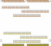
Game of connect the dots, anyone? :lol:
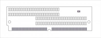
OK, I see what you're saying. Actually I'm cool with leaving the flash chips (and possibly an FPGA) on the SIMM as well and then putting other stuff in a FDD bay, or even something closer to what you described in your instructions (very nice detail, thanks, I get it!)
I think I'm going to have to leave the hardware hacking/testing for someone else to do though if they want I'd be glad to supply the bare SIMM PCB, the bare SIMM programmer PCB, and the SIMM socket...although I don't have any programmer PCBs available right now (they're on order and I think a Chinese holiday is just beginning so it'll be a while).
As for the height restrictions, I believe it was tt who said the current SIMM height is pretty close to the limit for what can fit into an SE/30. I'd imagine the SE/30 would be the one we have to look out for most. I know the IIci has plenty of clearance in every direction for the SIMM. I don't have any other ROM SIMM Macs available to look at, but I'd imagine we could make the PCB wider.
We have to keep in mind that level shifting is almost certainly going to be necessary as early as possible on the SIMM. This is going to add to the routing nightmare on the SIMM PCB. I like the idea of getting power from a Molex Y adapter (rather than the SIMM socket) as you said earlier.
I'd like to see a more community oriented project than me just making it all this time...I'm getting pretty worn out from circuit board design!
I think I'm going to have to leave the hardware hacking/testing for someone else to do though if they want
I'd be glad to supply the bare SIMM PCB, the bare SIMM programmer PCB, and the SIMM socket...although I don't have any programmer PCBs available right now (they're on order and I think a Chinese holiday is just beginning so it'll be a while).As for the height restrictions, I believe it was tt who said the current SIMM height is pretty close to the limit for what can fit into an SE/30. I'd imagine the SE/30 would be the one we have to look out for most. I know the IIci has plenty of clearance in every direction for the SIMM. I don't have any other ROM SIMM Macs available to look at, but I'd imagine we could make the PCB wider.
We have to keep in mind that level shifting is almost certainly going to be necessary as early as possible on the SIMM. This is going to add to the routing nightmare on the SIMM PCB. I like the idea of getting power from a Molex Y adapter (rather than the SIMM socket) as you said earlier.
I'd like to see a more community oriented project than me just making it all this time...I'm getting pretty worn out from circuit board design!
Speaking of community project, just so I know about such things, the 2MB ROM SIMM is in FreePCB format from the downloads section of the google code site, and the programmer PCB is in Eagle format:
http://code.google.com/p/mac-rom-simm-programmer/downloads/list
Have you gotten a chance to make the 8MB version available?
Would it make sense to check the files into the repo? They wouldn't be easily diffable, but the history and changelog would be there, and the repo might make it easier for collaboration.
I'd also like to say thanks for all the work you've done on this. Supporting other people and trying to meet their demands and expectations in your free time can be a wearing experience, and I'm very appreciative of your work on the project. You've not just created a useful project, you've enabled a whole new class of projects previously unobtainable.
http://code.google.com/p/mac-rom-simm-programmer/downloads/list
Have you gotten a chance to make the 8MB version available?
Would it make sense to check the files into the repo? They wouldn't be easily diffable, but the history and changelog would be there, and the repo might make it easier for collaboration.
I'd also like to say thanks for all the work you've done on this. Supporting other people and trying to meet their demands and expectations in your free time can be a wearing experience, and I'm very appreciative of your work on the project. You've not just created a useful project, you've enabled a whole new class of projects previously unobtainable.
Excellent idea, I hadn't thought of that before (checking the PCB files into the repository)! I'll try to do that soon. Especially now that Eagle 6 stores its files in an XML format, I think it will be easier to use in a repository.
I will upload the 8 MB SIMM design files soon. They are in Eagle format (once I figured out how to use Eagle, I realized it has much more capability than FreePCB [except for the fact that it's limited to 2 layers] )
P.S. I'm about halfway done implementing verify-while-writing capability. The GUI is either completely done or almost done, and the firmware is all that remains. Woohoo And thanks for your kind words--your software hacks enabled by the SIMM have been incredible too.
I will upload the 8 MB SIMM design files soon. They are in Eagle format (once I figured out how to use Eagle, I realized it has much more capability than FreePCB
[except for the fact that it's limited to 2 layers] )P.S. I'm about halfway done implementing verify-while-writing capability. The GUI is either completely done or almost done, and the firmware is all that remains. Woohoo
And thanks for your kind words--your software hacks enabled by the SIMM have been incredible too.Sounds like a good call. Feature creep is inevitable, and it usually makes more sense to go there if the additional features are an extension of building on previous work, such as going from 2MB to 8MB SIMMs. Hacking the ROM slot to have cables and daughter cards seems like a big shift in complexity and probably cost as well (and elegance). If something like that were to be done, then it probably is best to make a PDS card instead. I could see the FPGA and flash storage on ROM SIMM idea sort of being an extension, but also a big shift in complexity.
Yes, I'd like to also thank Doug and Rob for their contributions!!! I hope my posts haven't seemed too demanding, I'm just really excited about these developments, but I do really appreciate what everyone has done here. :b&w: Before this topic showed up here, I don't think we would have thought these new developments would have been a reality today. I can now boot my machine with more features/convenience and also have another area to tinker. This project has and will inspire and enable more hacking and discovery in the future.
Agreed, but wouldn't it be nice to change the ROM SIMM in an SE/30 without pulling the MoBo? :?:
If you'll recall, the Apple ][ world had an external expansion slot adapter that did exactly the same thing.