

Thread
Another IIci ROM hack
I don't really like stuff hanging off the machine, that's partially why I am stubbornly trying to adapt the PDS pass-through (another thread to come) on the Asante MacCon PDS card so I can have everything inside. Otherwise I would have gotten the ethernet/SCSI option. At the moment, I have the whole logic board outside the machine for testing ROMs and other hardware. Once it's more final (8MB Explorer ROM), I would want to just put it back together and not have to open it up too often.
For everyone's info I have updated the SIMM Programmer software to version 1.0.2. It includes support for verify while writing (requires another firmware update) and also lets you edit the read/write filenames manually in the main window.
Thanks to CC_333 we also have a version of 1.0.1 that works on OS X 10.4 (PPC or Intel). I'm not sure if he has tested it on a programmer board yet, but as long as I didn't do anything stupid with byte endianness (and I'm usually very careful about stuff like that), it should work fine on PPC. CC_333, would you mind making a new binary of version 1.0.2 and uploading it? The source code is on the repository--just use "git pull" to update your copy to the latest. I'll make it a featured download.
BTW, while adding the "verify while write" functionality, I learned a thing or two about port pins. If I didn't have a SIMM plugged in at all, it was passing the verification test. It turns out if you write a value to a pin, then read the pin back really fast (and nothing else writes to the pin in the meantime), it tends to stay at the same value you wrote to it. It's really undefined because nothing is driving the pin, but it tends to stay where you left it. So to remedy it, right before verifying, I write the opposite (NOT'ed) data to the data pins. This makes sure if the data is really valid, it will overwrite the opposite data that I left on it last. Weird, but understandable.
One more edit: the SIMM and programmer CAD files are now in the Google Code project repository. Anybody interested in doing anything with them (or the software, for that matter), let me know and I'll add you as a developer to the project!
Thanks to CC_333 we also have a version of 1.0.1 that works on OS X 10.4 (PPC or Intel). I'm not sure if he has tested it on a programmer board yet, but as long as I didn't do anything stupid with byte endianness (and I'm usually very careful about stuff like that), it should work fine on PPC. CC_333, would you mind making a new binary of version 1.0.2 and uploading it? The source code is on the repository--just use "git pull" to update your copy to the latest. I'll make it a featured download.
BTW, while adding the "verify while write" functionality, I learned a thing or two about port pins. If I didn't have a SIMM plugged in at all, it was passing the verification test. It turns out if you write a value to a pin, then read the pin back really fast (and nothing else writes to the pin in the meantime), it tends to stay at the same value you wrote to it. It's really undefined because nothing is driving the pin, but it tends to stay where you left it. So to remedy it, right before verifying, I write the opposite (NOT'ed) data to the data pins. This makes sure if the data is really valid, it will overwrite the opposite data that I left on it last. Weird, but understandable.
One more edit: the SIMM and programmer CAD files are now in the Google Code project repository. Anybody interested in doing anything with them (or the software, for that matter), let me know and I'll add you as a developer to the project!
Personally, the PDS, NuBus, DeclROM Slot Option is my first choice, but I've read both books and it's beyond the scope of what I can do. I didn't suggest breaking the entire ROM SIMM into the FDD bay, DQ misunderstood my intent and liked the notion of the down-n-dirtiest of implementations for the interface. I've got some experience with this kind of thing so I outlined the process for the test unit he poroposed.
I thought a Microcontroller with enough I/O to do a parallel interface to same in the FDD bay was the obvious jumpoff point in terms of NOT having anything hanging outside the case with the added ability to pop storage media in-n-out of the case from the most readily available of access points.
I'm not pushing the brute force expansion bay option for the ROMM SIMM, but without Microprocesser/FPGA/CPLD or AoG (act of God) support, that's the only thing I can do to help.
Barring someone developing a Declaration ROM for the Slot Manager way of doing things, dougg3's ROM expansion approach is the only way anything is going to get done at this point.
bbraun has backed off the DeclROM/board development path for need of PCB tools, design and testing support . . . as I understand his postings.
techknight is regrouping after exploring the 2.5" SCSI SSD Project microcontroller implementation, as I understood his posts regarding that great project.
BMOW appears to be off exploring new interests after his design ideas for a SD-card floppy emulator/Floppy Emu: an SD Card Floppy Emulator project threads.
trag is showing an enviable ability to concentrate on the most important things in life, family and the work that supports himself and his. You go guy! [ ] ]'>
] ]'>
That said:
The only thing I can think of offhand that might be worth looking into, now that ROM hacking is becoming possible, is really off the wall. Go figure. :
This has been a pet project of mine, for ten years now, for hacking the 2300. The T-REX ASIC, sits on the PBX bridged '030 bus of the PowerBooks: 190, 5300, and 1400. It's on the MoBo along with the PCMCIA Card Cage in the first two cases. T-REX is on a a very handy DaughterCard in the 1400, however, along with those same PCMCIA Slots that it supports along with the IR Talk hardware.
By tracing the 16bits of data and addressing back to PBX from T-REX, it should be easy enough to header the entire assembly to a PDS Card in the same way I've wanted to connect it to the Duo's full 32 bit, PBX bridged expansion Bus
It's my working assumption that the High and Low 16 bits of the PBX '030 bridge are split into the 16bit limited Video/EtherNet subsystems and the 16 bit limited PCMCIA/I/R-Talk subsystems of these PowerBooks.
1400s and their hinges are failing faster than ever these days and the T-REX Daughtercard is easily borrowed from a working specimen put into mothballs for safekeeping.
The question is: can we hack the ROMs of the earlier Macs to support PCMCIA, or is support for it already built into the very fabric of the NuBus/PDS-Slot Manager Architecture?
Dunno? :?:
I thought a Microcontroller with enough I/O to do a parallel interface to same in the FDD bay was the obvious jumpoff point in terms of NOT having anything hanging outside the case with the added ability to pop storage media in-n-out of the case from the most readily available of access points.
I'm not pushing the brute force expansion bay option for the ROMM SIMM, but without Microprocesser/FPGA/CPLD or AoG (act of God) support, that's the only thing I can do to help.
Barring someone developing a Declaration ROM for the Slot Manager way of doing things, dougg3's ROM expansion approach is the only way anything is going to get done at this point.
bbraun has backed off the DeclROM/board development path for need of PCB tools, design and testing support . . . as I understand his postings.
techknight is regrouping after exploring the 2.5" SCSI SSD Project microcontroller implementation, as I understood his posts regarding that great project.
BMOW appears to be off exploring new interests after his design ideas for a SD-card floppy emulator/Floppy Emu: an SD Card Floppy Emulator project threads.
trag is showing an enviable ability to concentrate on the most important things in life, family and the work that supports himself and his. You go guy! [
] ]'>That said:
The only thing I can think of offhand that might be worth looking into, now that ROM hacking is becoming possible, is really off the wall. Go figure. :
This has been a pet project of mine, for ten years now, for hacking the 2300. The T-REX ASIC, sits on the PBX bridged '030 bus of the PowerBooks: 190, 5300, and 1400. It's on the MoBo along with the PCMCIA Card Cage in the first two cases. T-REX is on a a very handy DaughterCard in the 1400, however, along with those same PCMCIA Slots that it supports along with the IR Talk hardware.
By tracing the 16bits of data and addressing back to PBX from T-REX, it should be easy enough to header the entire assembly to a PDS Card in the same way I've wanted to connect it to the Duo's full 32 bit, PBX bridged expansion Bus
It's my working assumption that the High and Low 16 bits of the PBX '030 bridge are split into the 16bit limited Video/EtherNet subsystems and the 16 bit limited PCMCIA/I/R-Talk subsystems of these PowerBooks.
1400s and their hinges are failing faster than ever these days and the T-REX Daughtercard is easily borrowed from a working specimen put into mothballs for safekeeping.
The question is: can we hack the ROMs of the earlier Macs to support PCMCIA, or is support for it already built into the very fabric of the NuBus/PDS-Slot Manager Architecture?
Dunno? :?:
FWIW, I've got custom, written from scratch, copyright free DeclROMs working, and a little library for POSIXy systems to assemble the ROM images. Pick your favorite Nubus or PDS card with a removable EPROM, and a custom DeclROM can be thrown on there. If a community project is stuck because a new DeclROM needs to be written, let me know.
Until a new card is made that needs one I don't think there's a whole lot that needs doing. Which is why I had made some motions about a PDS card with some flash on it, since that seemed like the lowest barrier to overcome.
I was also thinking about the limitations of what can be done in declrom vs. system ROM. Yesterday I wrote some PRAM modifying apps that enable/disable a feature of the AV ROMs that copies the ROM contents into RAM, and runs all ROM code from RAM that way, which kind of kicked off this idea.
Early in boot, the Slot Manager in the system ROM runs initialization code from the declrom in each card. To behave nicely, this should be <2K of code, and run within some timing constraints, a very limited environment, and maybe with interrupts disabled. The point is to just do early initialization of any hardware, video cards display their grey screen, etc. But, I'm kind of toying with the idea of whether it's feasible to just load your own system ROM (or copy the existing system ROM into RAM, and patch it on the fly, avoiding copyright issues) and never return to the original ROM. I'm kind of wondering if this might be what some accelerators might be doing.
Anyway, that wouldn't be able to do things like enable/disable ROM CRC checks, the POST RAM test, or the memory sizing change I did for the djMEMC machines, but it would allow mucking with the boot device selection process, loading new drivers, etc. Anyway, just an idea that'll be added to the end of a very long TODO list.
Until a new card is made that needs one I don't think there's a whole lot that needs doing. Which is why I had made some motions about a PDS card with some flash on it, since that seemed like the lowest barrier to overcome.
I was also thinking about the limitations of what can be done in declrom vs. system ROM. Yesterday I wrote some PRAM modifying apps that enable/disable a feature of the AV ROMs that copies the ROM contents into RAM, and runs all ROM code from RAM that way, which kind of kicked off this idea.
Early in boot, the Slot Manager in the system ROM runs initialization code from the declrom in each card. To behave nicely, this should be <2K of code, and run within some timing constraints, a very limited environment, and maybe with interrupts disabled. The point is to just do early initialization of any hardware, video cards display their grey screen, etc. But, I'm kind of toying with the idea of whether it's feasible to just load your own system ROM (or copy the existing system ROM into RAM, and patch it on the fly, avoiding copyright issues) and never return to the original ROM. I'm kind of wondering if this might be what some accelerators might be doing.
Anyway, that wouldn't be able to do things like enable/disable ROM CRC checks, the POST RAM test, or the memory sizing change I did for the djMEMC machines, but it would allow mucking with the boot device selection process, loading new drivers, etc. Anyway, just an idea that'll be added to the end of a very long TODO list.
The Radius Rocket writes the host's ROM to onboard RAM on the first boot and then boots from it for the, WHOOSSSHHHH!!!!!!!! re-boot.
Radius was licensed to do so, eliminating a major bottleneck, IDK of any other such ROMcopy to RAM offhand, outside the actual Macs, of course.
Radius was licensed to do so, eliminating a major bottleneck, IDK of any other such ROMcopy to RAM offhand, outside the actual Macs, of course.
I just pulled out the datasheet for the Atmel AT90USB647:
So the port values in fact affect the pull-up resistors when in the input direction. I would recommend writing all 1s to the ports to activate the pull-ups when reading. This should return all 1s whenever polling the ports with no SIMM inserted. Then just use the PINx registers to read the input values. This differs from other microcontrollers - I am used to using the PORTx registers for both reading and writing data.
Thanks for the suggestion Dennis Nedry! I'm well aware of the pull-ups and their register layout and everything. I actually tried turning the pull-ups on at first, but it only fixed the problem on the 16 pins that are controlled through my GPIO expander chip--the 16 pins controlled by the AVR still had problems. I figured the AVR pull-ups just weren't responding fast enough and moved on to my other technique. (I now realize I was wrong...)
When you reminded me that the PORT bits are what control the pull-ups (I knew that but I made my own library routines that do it for me so I wasn't thinking about the register layout at all), you jogged my memory. The reason it worked on the GPIO expander was because it has a separate pull-up enable register. I was only configuring the pull-ups at the start of the program, so the AVR's pull-ups were getting changed around every time I wrote data to the chips (but the GPIO expander's pull-ups were being left alone -- that's why it worked on them). I just changed the code to disable the weird inverted write, and instead ensure all pull-ups are enabled on every read cycle, and now it works fine. This also has the effect of making the chip ID sequence return 0xFF when a chip is not present (instead of 0x90, which is the last byte I write to the chips to initiate the identification sequence). I was wondering why it was doing that, but it never bothered me enough to think about it).
It all makes sense now! And I feel foolish. In my next firmware release I'll probably use the technique you listed instead, so everything will have a defined value of all 1s as you mentioned. Thanks again!
When you reminded me that the PORT bits are what control the pull-ups (I knew that but I made my own library routines that do it for me so I wasn't thinking about the register layout at all), you jogged my memory. The reason it worked on the GPIO expander was because it has a separate pull-up enable register. I was only configuring the pull-ups at the start of the program, so the AVR's pull-ups were getting changed around every time I wrote data to the chips (but the GPIO expander's pull-ups were being left alone -- that's why it worked on them). I just changed the code to disable the weird inverted write, and instead ensure all pull-ups are enabled on every read cycle, and now it works fine.
This also has the effect of making the chip ID sequence return 0xFF when a chip is not present (instead of 0x90, which is the last byte I write to the chips to initiate the identification sequence). I was wondering why it was doing that, but it never bothered me enough to think about it).It all makes sense now! And I feel foolish.
In my next firmware release I'll probably use the technique you listed instead, so everything will have a defined value of all 1s as you mentioned. Thanks again!I see now... I thought you meant some external box like an ExpanSE (sp?) the Nubus expansion chassis, though I wouldn't mind having that dangling off the machine if it worked with normal cards. It sounds like the ROM transfer rate wouldn't be too much faster than SCSI, so one option available now is to mount an Artmix CF/SCSI board in the FDD bay and stick A CF card through the floppy slot.
We should quantify ROM vs. paged ROM vs. RAM vs. SCSI vs. NuBus speeds. If you can get the data there fast enough (i.e. parallel ROM like dougg3's current designs), ROM should be the fastest but by how much I'm not sure.
Everyone loves to argue about benchmarks. CF speed benchmarks seems to be one of this forum's favorite things to argue about. But, we may as well argue over actual data instead of theoreticals, right?
Over lunch I wrote this set of tests. I am by no means a qualified benchmark writer, but I'll give it a go anyway.
The 3 tests involve copying data, in 256KB chunks read a long word at a time, into RAM, then flushing the data cache, and doing it again in a loop 1000 times. The 3 tests are doing this from RAM to RAM, ROM to RAM, and Slot to RAM. The slot test is using the slot manager to find a card then directly read the last 256KB from the card's standard address space, which is where the declrom lives. It just takes the first non-zero slot it finds.
Sources are included, so feel free to inspect what is going on, make changes, etc.
I ran it on a 660av with a nubus adapter populated with a video card, and a IIx with a nubus video card. Both video cards were being used as the active head for the machine.
If the test is run for longer (there's an ITERATIONS macro at the top of the source file), the gap between ROM and RAM speeds becomes more noticeable.
And just to throw more ideas into this pot, thinking about tt's idea for custom SIMMs, I'd be interesting to see if we can still address something in the SIMM slot, even if the memory controller has not recognized it as RAM. I'm thinking of the Sun SS20, which takes nonvolatile storage for disks, and a framebuffer in its DIMM slots.
Over lunch I wrote this set of tests. I am by no means a qualified benchmark writer, but I'll give it a go anyway.
The 3 tests involve copying data, in 256KB chunks read a long word at a time, into RAM, then flushing the data cache, and doing it again in a loop 1000 times. The 3 tests are doing this from RAM to RAM, ROM to RAM, and Slot to RAM. The slot test is using the slot manager to find a card then directly read the last 256KB from the card's standard address space, which is where the declrom lives. It just takes the first non-zero slot it finds.
Sources are included, so feel free to inspect what is going on, make changes, etc.
I ran it on a 660av with a nubus adapter populated with a video card, and a IIx with a nubus video card. Both video cards were being used as the active head for the machine.
Code:
660av:
Starting RAM test
RAM test copied 250 MB in 26 seconds
Starting ROM test
ROM test copied 250 MB in 27 seconds
Testing Slot: e
Address: fe000000
Address: fefbffff
Slot test copied 250 MB in 324 seconds

IIx:
Starting RAM test
RAM test copied 250 MB in 48 seconds
Starting ROM test
ROM test copied 250 MB in 48 seconds
Testing Slot: 9
Address: f9000000
Address: f9fbffff
Slot test copied 250 MB in 143 secondsAnd just to throw more ideas into this pot, thinking about tt's idea for custom SIMMs, I'd be interesting to see if we can still address something in the SIMM slot, even if the memory controller has not recognized it as RAM. I'm thinking of the Sun SS20, which takes nonvolatile storage for disks, and a framebuffer in its DIMM slots.
Oh, one other thing about the ROM accesses. Only the first 1MB of ROM is mapped into 24bit address space, so anything beyond that will need to be 32bit accesses. Which means an addressing mode swap before and after accesses. So the above is kind of a best case on ROM access times.
Well, I played with the RAM thing a bit on a IIx.
Out of the box, the mac plays the bad chimes if you have an invalid memory configuration (one simm in a bank of 4, in the IIx). So, I patched out the check. Then, the MMU setup is only mapping in the RAM that was detected, and setting up a memory hole and then mirroring the RAM all the way up to 0x40000000. The single simm wasn't included in the detected RAM (this is good, we don't want it added to available memory), so wasn't included in what was mapped in. I was able to patch in a hard coded chunk, but it seems the GLU decoder is generating a bus error when trying to access that range.
So, I didn't have much luck with abusing the RAM slots.
I used the new SIMM Programmer for this with the 8MB SIMM, and the verify while writing is very cool. Thanks dougg3!
Out of the box, the mac plays the bad chimes if you have an invalid memory configuration (one simm in a bank of 4, in the IIx). So, I patched out the check. Then, the MMU setup is only mapping in the RAM that was detected, and setting up a memory hole and then mirroring the RAM all the way up to 0x40000000. The single simm wasn't included in the detected RAM (this is good, we don't want it added to available memory), so wasn't included in what was mapped in. I was able to patch in a hard coded chunk, but it seems the GLU decoder is generating a bus error when trying to access that range.
So, I didn't have much luck with abusing the RAM slots.
I used the new SIMM Programmer for this with the 8MB SIMM, and the verify while writing is very cool. Thanks dougg3!
Hmm, well it is a very interesting idea, is the GLU decoder sort of an untouchable black box?
The benchmarks look pretty good, nice work! BTW, I couldn't download the program.
The benchmarks look pretty good, nice work!
BTW, I couldn't download the program.
Sorry the download should be fixed, I had the path wrong, but fixed now.
If there's a software solution for this bus error, it has exceeded my patience for the time being.
If there's a software solution for this bus error, it has exceeded my patience for the time being.
There's precedent for abusing RAM, the only internal Video Adapter ever made for the PowerBook 100 used the RAM interface as its wedge into the I/O structure.
Re: Microcontroller vs. FPGA
I think that an FPGA will just work better in every way. The only disadvantage of using an FPGA is that folks who are likely to help also probably have more experience with microcontrollers. Oh, and microcontroller development systems are (usually) less expensive, but that's a one-off purchase for anyone developing. Doug's analysis of data rates is salient. It is difficult to have a microcontroller keep up with the I/O and still do other useful work, especially at the speeds typically available.
An FPGA can have several blocks all operating simultaneously, accomplishing the many contemporaneous tasks required.
Re: PCB Software:
I am not familiar with KiCAD. What are the benefits of using it? I like and have used Osmond PCB, which is not free, but the only limitation on the free download is the ability to output data in fabrication format (PDF and Gerber). For collaborators, if some of them are really broke, only one person would need the paid version, which I have. However, in my experience, the auto-routing is not very good, so if KiCAD has good auto-routing....
Osmond runs on the Mac and there is a System 8 and System 9 version available as well as versions for 10.4 and 10.5. Also, Mr. Chavez has always been super responsive to any emails about his product. I hit a bug one time, sent him before and after saves of my board where the bug was occurring, and he identified the bug and had a fix out within a couple of days. He's been developing this for ten years or so.
http://www.osmondpcb.com/index.html
http://www.osmondpcb.com/download.html
Re: USB on a SIMM
Take a look at this chip:
http://www.nxp.com/products/interface_and_connectivity/usb_host_controllers/SAF1760BE.html
Hmmm, seems hard to find. Or this chip:
http://www.ftdichip.com/Support/Documents/DataSheets/ICs/DS_Vinculum-II.pdf
This is a USB host controller with a configurable microprocesser interface (instead of PCI), 16 and 32 bit selectable, and PIO and DMA selectable. The nxp package is 128 pins (routing nightmare) in a 23 X 17 mm package.
I think an achievable goal might be to build a ROM SIMM with this chip on it and a USB port or two. The USB ports will probably need to be at the end of wires which solder to the card, as there's probably not room on the card for actual USB sockets.
Write the USB driver to only support mass storage, at least at first. That will get USB sticks into the Mac as storage devices.
The board would almost certainly have to be four or more layers to handle the routing. I would suggest using the Flash chips Doug has in 16bit wide mode, putting two of them on one side, and using the other side of the board and the rest of the space for the USB circuitry.
And, as Doug surmised, it would need level shifters for the I/Os. I/O only goes up to 3.3V although it will run off of a 5V supply.
Anyway, I think this might be an interesting first project, which probably would not require an FPGA or CPLD, although without doing a thorough analysis, I'm not sure it would interface to the 68030 bus gluelessly. Probably need a small PLD at least to decode the addresses to a couple of Chip Enables.
I have considered interfacing this chip to a 68K Macintosh before, but the lack of anyone to write drivers always stopped me.
Re: Super Duper Do Everything Project
Start with this Xilinx Spartan 3AN Development Board ($200):
http://www.xilinx.com/products/boards-and-kits/HW-SPAR3AN-SK-UNI-G.htm
Which, if I read correctly is also the one Bigmessofwires used to build his Mac 512 hardware emulator. If we could get him to help...
http://68kmla.org/forums/viewtopic.php?p=158134#p158134
The cool thing about this development board is that the FPGA code to support the DDR2 chip and Flash, and VGA port and 10/100 ethernet is already written. All that's really needed is to interface those components with the Macintosh bus.
Build a circuit board to interface between the development board's I/Os and the PDS slot of the Macintosh. Use the existing devices on the development board and the FPGA code which comes from Xilinx to drive them and then write code to interface those devices to the Macintosh PDS slot interface.
Ultimately, we would do our own board with the desired devices, but this would kick development off quickly, which is what a development board is meant to do...
The development board has DDR2 memory, parallel flash, Serial Flash, and 10/100 ethernet with PHY. Also crude VGA video out.
There is no USB however (well a slave interface for programming the board, but no host).
The Xilinx XC3S700AN chip alone costs about $40 each and has the blocks and I/O pins to do anything we could ever imagine. However, it is a BGA part, so soldering it down is problematical.
But I've looked at the QFP options, and generally, by the time you've interfaced them to the Macintosh bus, there just aren't enough I/O pins left to do very much cool stuff.
See this thread, if you have the patience for it...
http://68kmla.org/forums/viewtopic.php?p=156907#p156907
and these:
http://68kmla.org/forums/viewtopic.php?p=155790#p155790
http://68kmla.org/forums/viewtopic.php?p=156600#p156600
http://68kmla.org/forums/viewtopic.php?p=60709#p60709
http://68kmla.org/forums/viewtopic.php?p=60790#p60790
Re: Time
I'd love to work on either the USB SIMM or the full bore FPGA development kit interface idea, but
I think that an FPGA will just work better in every way. The only disadvantage of using an FPGA is that folks who are likely to help also probably have more experience with microcontrollers. Oh, and microcontroller development systems are (usually) less expensive, but that's a one-off purchase for anyone developing. Doug's analysis of data rates is salient. It is difficult to have a microcontroller keep up with the I/O and still do other useful work, especially at the speeds typically available.
An FPGA can have several blocks all operating simultaneously, accomplishing the many contemporaneous tasks required.
Re: PCB Software:
I am not familiar with KiCAD. What are the benefits of using it? I like and have used Osmond PCB, which is not free, but the only limitation on the free download is the ability to output data in fabrication format (PDF and Gerber). For collaborators, if some of them are really broke, only one person would need the paid version, which I have. However, in my experience, the auto-routing is not very good, so if KiCAD has good auto-routing....
Osmond runs on the Mac and there is a System 8 and System 9 version available as well as versions for 10.4 and 10.5. Also, Mr. Chavez has always been super responsive to any emails about his product. I hit a bug one time, sent him before and after saves of my board where the bug was occurring, and he identified the bug and had a fix out within a couple of days. He's been developing this for ten years or so.
http://www.osmondpcb.com/index.html
http://www.osmondpcb.com/download.html
Re: USB on a SIMM
Take a look at this chip:
http://www.nxp.com/products/interface_and_connectivity/usb_host_controllers/SAF1760BE.html
Hmmm, seems hard to find. Or this chip:
http://www.ftdichip.com/Support/Documents/DataSheets/ICs/DS_Vinculum-II.pdf
This is a USB host controller with a configurable microprocesser interface (instead of PCI), 16 and 32 bit selectable, and PIO and DMA selectable. The nxp package is 128 pins (routing nightmare) in a 23 X 17 mm package.
I think an achievable goal might be to build a ROM SIMM with this chip on it and a USB port or two. The USB ports will probably need to be at the end of wires which solder to the card, as there's probably not room on the card for actual USB sockets.
Write the USB driver to only support mass storage, at least at first. That will get USB sticks into the Mac as storage devices.
The board would almost certainly have to be four or more layers to handle the routing. I would suggest using the Flash chips Doug has in 16bit wide mode, putting two of them on one side, and using the other side of the board and the rest of the space for the USB circuitry.
And, as Doug surmised, it would need level shifters for the I/Os. I/O only goes up to 3.3V although it will run off of a 5V supply.
Anyway, I think this might be an interesting first project, which probably would not require an FPGA or CPLD, although without doing a thorough analysis, I'm not sure it would interface to the 68030 bus gluelessly. Probably need a small PLD at least to decode the addresses to a couple of Chip Enables.
I have considered interfacing this chip to a 68K Macintosh before, but the lack of anyone to write drivers always stopped me.
Re: Super Duper Do Everything Project
Start with this Xilinx Spartan 3AN Development Board ($200):
http://www.xilinx.com/products/boards-and-kits/HW-SPAR3AN-SK-UNI-G.htm
Which, if I read correctly is also the one Bigmessofwires used to build his Mac 512 hardware emulator. If we could get him to help...
http://68kmla.org/forums/viewtopic.php?p=158134#p158134
The cool thing about this development board is that the FPGA code to support the DDR2 chip and Flash, and VGA port and 10/100 ethernet is already written. All that's really needed is to interface those components with the Macintosh bus.
Build a circuit board to interface between the development board's I/Os and the PDS slot of the Macintosh. Use the existing devices on the development board and the FPGA code which comes from Xilinx to drive them and then write code to interface those devices to the Macintosh PDS slot interface.
Ultimately, we would do our own board with the desired devices, but this would kick development off quickly, which is what a development board is meant to do...
The development board has DDR2 memory, parallel flash, Serial Flash, and 10/100 ethernet with PHY. Also crude VGA video out.
There is no USB however (well a slave interface for programming the board, but no host).
The Xilinx XC3S700AN chip alone costs about $40 each and has the blocks and I/O pins to do anything we could ever imagine. However, it is a BGA part, so soldering it down is problematical.
But I've looked at the QFP options, and generally, by the time you've interfaced them to the Macintosh bus, there just aren't enough I/O pins left to do very much cool stuff.
See this thread, if you have the patience for it...
http://68kmla.org/forums/viewtopic.php?p=156907#p156907
and these:
http://68kmla.org/forums/viewtopic.php?p=155790#p155790
http://68kmla.org/forums/viewtopic.php?p=156600#p156600
I looked at doing something similar with the 68030 processor, and it turns out to be either a pain or expensive, or both to find usable cabling for such a project. At least that was my conclusion. You're considering fewer signals, so it might be more doable, but by the time you build an off-SIMM board, I think you might as well go full PDS slot.
http://68kmla.org/forums/viewtopic.php?p=60709#p60709
http://68kmla.org/forums/viewtopic.php?p=60790#p60790
Re: Time
I'd love to work on either the USB SIMM or the full bore FPGA development kit interface idea, but
Coaching my son's Fall Baseball team right now. Then PEX DIMM. Then, maybe... You guys are way more energetic on this stuff than I can manage. I hope some of my past ramblings/conceptual designs are helpful.trag is showing an enviable ability to concentrate on the most important things in life, family and the work that supports himself and his. You go guy! [
Interesting notion:
1. If we're powering my ROM SIMM extender cable from a Molex Y Adapter, this frees up a considerable number of pins for the adapted SIMM Slot.
2. None of the targeted Macs have DMA, as I understand it, this means the mac cannot be using the Bank, Row or Chip Select lines of System Memory at the same time we're banging on the ROM SIMM. Neh?
3. Pins 1,13 and 46 become redundant +5V sources and Pins 10, 30 and 64 become redundant Ground lines as well.
4. Patch wiring the proper lines from the System Memory Bank Subsystem to the extender card could allow for a HUGE VM SPACE becoming addressable given the correct system patch/driver, would it not?
< . . . HEH! HEH! HEH! } . . . >
1. If we're powering my ROM SIMM extender cable from a Molex Y Adapter, this frees up a considerable number of pins for the adapted SIMM Slot.
2. None of the targeted Macs have DMA, as I understand it, this means the mac cannot be using the Bank, Row or Chip Select lines of System Memory at the same time we're banging on the ROM SIMM. Neh?
3. Pins 1,13 and 46 become redundant +5V sources and Pins 10, 30 and 64 become redundant Ground lines as well.
4. Patch wiring the proper lines from the System Memory Bank Subsystem to the extender card could allow for a HUGE VM SPACE becoming addressable given the correct system patch/driver, would it not?
< . . . HEH! HEH! HEH! }
. . . >
i want one for my IIsi.
Man it would be great to boot Mac os image, with out a HD,
load my IIsi up with ram, do the Rom to Ram boot option,
maybe add a boot key that sits there and plays super mario theme
sounds like a heap of fun to me,
Man it would be great to boot Mac os image, with out a HD,
load my IIsi up with ram, do the Rom to Ram boot option,
maybe add a boot key that sits there and plays super mario theme
sounds like a heap of fun to me,
I was reading in another thread about hacking the ROM in the Quadra so it could use 256MBs of RAM (2x128MBs.) Could the same be done for the IIci? Stick in 8 32MB SIMMs? I don't know what I'd do with 256MBs of RAM, but it sounds like silly fun.
I'm a total newbie on the hardware side. More than a decade ago I took some lower division digital logic classes, and that's been about it. But hey, I'm willing to give it a shot.
So, I have nothing for or against KiCAD and hadn't heard of Osmond PCB before. I had heard of FreePCB, Eagle, and KiCAD had showed up on a google search. I started messing around with the free version of Eagle and really enjoyed the parts library. The reason I started looking at other solutions was the hobby edition is limited to 160mmx100mm. For an 030 PDS slot using the 120 pin connector, that's about 120mm on its own. I'm sure that'd be plenty of space for someone more experienced, but I was looking at DIP parts because I can actually solder them, and that eats a lot of PCB space. It looks like the Professional edition of Eagle allows 4mx4m boards, but costs $1700. Which isn't exactly pocket change, but I'm starting to think isn't that bad...
KiCAD and OsmondPCB look good to me for the simple reason that they run on OSX. I have a Win7 VM, but I find the experience of doing actual work within the VM to be less than enjoyable. However, the first thing I want to do is add the 120pin PDS connector, which no one other than Eagle seems to have in their parts library. I go to create the part, and it comes up with a window for me to manually create each pin individually and freehand lay out the spacing on the grid for 120 pins. I see that and then go back to Eagle and start to wonder how much my time an sanity are worth.
But like I said, I'm all new to this, and it's entirely possible I'm missing something.
128MB of RAM is a hardware limitation of the memory controller in the IIci. 30 pin SIMMs have 12 address lines. The address is multiplexed (the address lines are used twice, once for row, once for column) so the addressable space on a 30 pin SIMM is 12 X 2 = 24 bits. 24 bits of address space gives 2^24 addresses => 16 Million addresses.I was reading in another thread about hacking the ROM in the Quadra so it could use 256MBs of RAM (2x128MBs.) Could the same be done for the IIci? Stick in 8 32MB SIMMs? I don't know what I'd do with 256MBs of RAM, but it sounds like silly fun.
The 30 pin SIMM is 1 byte wide. It supplies 8 bits of data (or writes 8 bits of data) at a time. 16 million addresses times 1 byte width equals 16 MB of capacity.
So the largest possible capacity for a 30 pin SIMM is 16 MB. There are no additional address lines available to expand its hardware capacity.
Now, all that said, it might be possible to build some kind of hardware device which maps more memory into the IIci's address space, but the physical memory for it would have to live on a card, such as a NuBus or PDS card.
Well it is a bit of a pain to create new parts, but once they're created, the work is done.However, the first thing I want to do is add the 120pin PDS connector, which no one other than Eagle seems to have in their parts library. I go to create the part, and it comes up with a window for me to manually create each pin individually and freehand lay out the spacing on the grid for 120 pins. I see that and then go back to Eagle and start to wonder how much my time an sanity are worth.
But like I said, I'm all new to this, and it's entirely possible I'm missing something.
For example, I have a 64 pin SIMM edge connector in my Osmond Library which I laid out. There's no reason for me to remake all those pads every time I draw a IIfx or ROM SIMM.
Anyway, here's what I would do (from memory, so I'm probably leaving out details; there's a pretty good tutorial with a section on creating parts).
First look over the dimensions of the 120 pin connector. Then launch Osmond. Click on the Create Part button. Set the snap to grid to something that makes sense given the spacing of the connector's pins. Pick out the appropriate sized through hole/via. Check your labeling. Osmond will automatically increment the label number, so it saves time to do this up front so all your pin holes get the numbers/labels you want on the part.
Then lay out the through holes/vias on the grid in the order that makes sense. It really shouldn't take very long if you use the snap to grid to help.
Then draw an outline of the physical connector housing on the silk screen layer. Add a label you might like to have appear when you add the part to a board. And save the part.
Or something like that. It'll probably take two or three tries to get it just right the first time, but each try should not take more than ten or fifteen minutes, especially if you work through the Osmond Tutorial first.
Thanks! On the last page of the tutorial, it shows the format for parts and net lists. That was a major breakthrough for me. It's a very simple text file, and I can configure all the pins, give them names, define the part name from the part type, and then configure connections, giving each connection a name, all with text files. That's something I'm way more comfortable with.
I was able to define the EuroDIN120 in a couple minutes from that, and connect up data and address signals to a 29F040 in a couple more.
Since I'm brand new to all this, I'm taking baby steps. My initial goal is 030 PDS to a single 29F040 flash chip. That's only 8 bits of data, but the slot manager is more than happy to work with limited byte lanes (practically all nubus and pds cards have a single 27C256 as their declrom), so simplest that still works is great.
For addressing, I was just going to use 7404's and 7408's to NOT A24 and A26, then AND those with A25, A27, & A28-A31, to get accesses to 0xFA0000000, being standard slot space for slot A. Then connect that to /OE. /WE and /CE to VCC.
I got an extra burst of motivation this evening and attempted to wire it up:
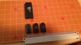
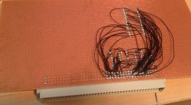
But, I put it in a IIsi and nothing. The machine boots fine, just nothing there. I poked around with macsbug, and there's nothing in slot A's address space.
Oh well. I managed to create quite a rat's nest in there.
I was able to define the EuroDIN120 in a couple minutes from that, and connect up data and address signals to a 29F040 in a couple more.
Since I'm brand new to all this, I'm taking baby steps. My initial goal is 030 PDS to a single 29F040 flash chip. That's only 8 bits of data, but the slot manager is more than happy to work with limited byte lanes (practically all nubus and pds cards have a single 27C256 as their declrom), so simplest that still works is great.
For addressing, I was just going to use 7404's and 7408's to NOT A24 and A26, then AND those with A25, A27, & A28-A31, to get accesses to 0xFA0000000, being standard slot space for slot A. Then connect that to /OE. /WE and /CE to VCC.
I got an extra burst of motivation this evening and attempted to wire it up:
But, I put it in a IIsi and nothing. The machine boots fine, just nothing there. I poked around with macsbug, and there's nothing in slot A's address space.
Oh well. I managed to create quite a rat's nest in there.
Hey, cool idea for a test! I saw you said you connected /CE to VCC--just to double check, you did mean GND right? Otherwise the chip won't respond.
BTW, although I don't design PCBs as part of my job, some of my coworkers do. From what I've gleaned, it's pretty standard to have to make your own components for things the software doesn't already include. A necessary evil I guess you can say...
BTW, although I don't design PCBs as part of my job, some of my coworkers do. From what I've gleaned, it's pretty standard to have to make your own components for things the software doesn't already include. A necessary evil I guess you can say...
Nice job of it, bb! It's great to see you back on this line of research. :approve:
I don't like wire wrap either, but it's a lot easier to undo/redo for degubbing your board. Did you print a mirrored copy of your board layout to go by for wiring from the "wrong" side?
I don't like wire wrap either, but it's a lot easier to undo/redo for degubbing your board. Did you print a mirrored copy of your board layout to go by for wiring from the "wrong" side?
If anyone needs any NuBUS or PDS connectors to play with, or chip sockets, or SIMM sockets, or anything else, I think there might be some at my local electronics store. If you give me a list of what you need, I can find out.
Straight up wire wrap sockets for PDS and NuBus would be a big help for my SuperIIsi™ project. Some ROM SIMM Sockets for the extension cable project would be fabulous.
Speaking of which: DQ, you wouldn't have any reject programmer boards on hand would you? I don't need a functional board for the feasibility study, just the patchable thru-holes/connections between the header pads and SIMM connectors.
Heh, come to think of it, just a bare reject SIMM Board and SIMM Connector would be good enough for an indescribably fugly, minimalist, but workable test cable. [}] ]'>
Speaking of which: DQ, you wouldn't have any reject programmer boards on hand would you? I don't need a functional board for the feasibility study, just the patchable thru-holes/connections between the header pads and SIMM connectors.
Heh, come to think of it, just a bare reject SIMM Board and SIMM Connector would be good enough for an indescribably fugly, minimalist, but workable test cable. [}
] ]'>Good catch Doug. Also, your logic for decoding /OE... You'll want that to have a low result on valid addresses and a high result otherwise. The /OE, /CE and /WE are all active on low/ground.
Finally, double check the datasheet for the Flash you're using. Some of them have a /Reset pin which must be held high in order to access the chip. If you leave it floating, the chip usually just stays in reset. This bit me on the AT29F800, IIRC. Not all Flash have a /Reset pin, but some do.
You can decode the address range 0xFAXXXXXX with 2 chips if you have a 7400 (quad 2-input NAND) and a 7432 (quad 2-input OR). This leaves one extra NAND gate.
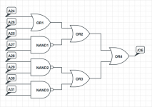
Note that in Dennis's diagram, the address lines from top to bottom are 24, 26, 25, 27, 28, 29...
The swapping of 25 and 26 is kind of critical to making the circuit work.
The swapping of 25 and 26 is kind of critical to making the circuit work.