

Thread
Another IIci ROM hack
jt, to answer your thickness question.
The old SIMM thickness is .050" or maybe .047". Typical PCB or copper clad board, these days, is .063" or maybe .0625", whic his also modern DIMM thickness, I think.
The SIMM sockets of yore have pins on both sides, even though the pads on opposite sides of the SIMM are common with each other. So it doesn't really matter which side you grind down, as long as one side is still available to make contact with the socket pins.
Grinding the pads off of one side of the board can't be good for reliability though. It's better to get the proper thickness copper clad board in the first place. Are you in imminent danger of etching something yourself? With the prices at Seed Studio, you're almost always going to be better off using them. Especially since making vias is a time consuming, finicky pain.
The old SIMM thickness is .050" or maybe .047". Typical PCB or copper clad board, these days, is .063" or maybe .0625", whic his also modern DIMM thickness, I think.
The SIMM sockets of yore have pins on both sides, even though the pads on opposite sides of the SIMM are common with each other. So it doesn't really matter which side you grind down, as long as one side is still available to make contact with the socket pins.
Grinding the pads off of one side of the board can't be good for reliability though. It's better to get the proper thickness copper clad board in the first place. Are you in imminent danger of etching something yourself? With the prices at Seed Studio, you're almost always going to be better off using them. Especially since making vias is a time consuming, finicky pain.
Are you making a daughter board or extending a stock ROM SIMM?
The way I understand it, is that I'm taking the very low road to test the feasibility of moving the programmed ROM SIMM from the socket on the mobo to the socket on a card in the FDD bay. DQ seems to be exploring the high road possibility of using an FPGA to connect to additional neat stuff, whether on a larger(?) ROM SIMM or on the end of a cable as I had suggested.
Real estate on an enlarged ROM SIMM will be severely limited, especially for the SE/30 crowd. Moving additional circuitry, even the ROMs themselves to the FDD Bay seems like the best choice to me. If we're gonna do an SD Card or any other modern, removable I/O hack, having it near the FDD Slot is a no-brainer as far as I'm concerned.
The graphic that got you laughing is the current iteration of the dummy SIMM end of the extender.
This one gives a better picture of the two halves, the board will be cut cut across the middle.
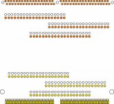
When I did this quick study, I thought I'd need to use three standard IDE cables and headers for them at each end of the testing units. When I researched the newer ATA cabling, I cut it down to two connectors/board. I'm going to take a nap and fire up Illustrator 8 again tonight.
1) Move the dip plug sockets together and lower on the board to bring it in line with DQ's ROM SIMM form factor.
2) Continue the traces on to the Dip Plug sockets and SIMM Slot end of the extender Cable.
3) Continue those traces on to a 64 position machine pin socket for homebrew programmer adapter development.
4) Continue those traces on to sockets for:
________ the yet to be identified DuoDock ROMs . . .
________ the PLCC ROMs for the MiniDock and my Radius VidCards . . .
________ bbraun's suggested EEPROM package . . .
________ the 28pin EPROMs used on most early Cards and peripherals . . .
________ whatever other suggestions come up . . .
________ and just maybe . . . the friggin' kitchen sink! [ )] ]'>
Other than some patch wiring for the adapter connections, It's pretty much a single sided board that doesn't need any plated thru holes . . .
. . . should get three sets ganged on a 12'" x 12" blank . . .
. . . dunno, we'll see, I've got a couple more notions rattling betwixt the earlobes, ATM. :scrambled:
Real estate on an enlarged ROM SIMM will be severely limited, especially for the SE/30 crowd. Moving additional circuitry, even the ROMs themselves to the FDD Bay seems like the best choice to me. If we're gonna do an SD Card or any other modern, removable I/O hack, having it near the FDD Slot is a no-brainer as far as I'm concerned.
The graphic that got you laughing is the current iteration of the dummy SIMM end of the extender.
This one gives a better picture of the two halves, the board will be cut cut across the middle.
When I did this quick study, I thought I'd need to use three standard IDE cables and headers for them at each end of the testing units. When I researched the newer ATA cabling, I cut it down to two connectors/board. I'm going to take a nap and fire up Illustrator 8 again tonight.
1) Move the dip plug sockets together and lower on the board to bring it in line with DQ's ROM SIMM form factor.
2) Continue the traces on to the Dip Plug sockets and SIMM Slot end of the extender Cable.
3) Continue those traces on to a 64 position machine pin socket for homebrew programmer adapter development.
4) Continue those traces on to sockets for:
________ the yet to be identified DuoDock ROMs . . .
________ the PLCC ROMs for the MiniDock and my Radius VidCards . . .
________ bbraun's suggested EEPROM package . . .
________ the 28pin EPROMs used on most early Cards and peripherals . . .
________ whatever other suggestions come up . . .
________ and just maybe . . . the friggin' kitchen sink! [
)] ]'>Other than some patch wiring for the adapter connections, It's pretty much a single sided board that doesn't need any plated thru holes . . .
. . . should get three sets ganged on a 12'" x 12" blank . . .
. . . dunno, we'll see, I've got a couple more notions rattling betwixt the earlobes, ATM. :scrambled:
I see... sounds like a good idea for a feasibility study. I'm not knocking any ideas around here, most experiments have the potential lead to new discoveries or ideas. :b&w:
The extender could also relate to the idea of extending the CPU socket or PDS slot for the Daystar crowd, right?
The extender could also relate to the idea of extending the CPU socket or PDS slot for the Daystar crowd, right?
Dunno . . . it's na . . . zzzzzzzzzzzzzzzzzzzzzzzzzzzzzzzzzzzzzzzzzzzzzzzzzzz
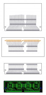
Ok, gang, here's the concept study for the extender project as it now stands.
Criricism-n-suggestions of every type are encouraged and will be much appreciated. :approve:
Input signal flow is represented in the diagram as from bottom to top and each cards is shown as a discrete unit. The actual layout is still single sided. for a one of the three ganged cards in a row of the three triplets on the 12" x 12" copper clad FRP from CrapShack I'm still hoping to find in one of the boxen. The top card will be rotated 180 degrees so the edgecard connectors are on the opposing side of those on the bottom card. Other sourcing suggestions for inexpensive fab on a one square foot, max size, blank will be considered.
______________________________________________________________________________________________________
The top card is a parallel, peripherally related, development that's a gimme in the production process. It's intended to make adapting dougg3's programmer board for use in building "standard" format adapters for individual or ganged ROMs in alternate IC packaging by the traditional process. The loose traces will lead to the four different socket types discussed earlier, wire wrap or soldered patch wiring will be necessary unless I move to a double sided, plated thru hole process on a blank of the proper thickness. I'm assuming that this will be prohibitively expensive, prove me wrong PLEASE!. Funds for the toy account are unbelievably tight for the moment. I also don't like the idea of learning to run a real PCB Design App, but doing so for the three cards individually ought to be doable with the free version of just about any program if it comes to that. My brain's PFPGA is burned in or the Adobe Illustrator graphic arts approach, which it perfect for my homebrew PCB fab processes.
______________________________________________________________________________________________________
The other pair of cards are the extender boards, the main line of development. They'll be connected by standard IDC DIP Plugs in the sockets on the boards. The DIP plugs will be hacked to achieve alternate ground lines on a doubled cable mod during the ribbon cable punchdown process. Description of hack above. I may or may not flip the signals on one to equalize cable/signal runs for timing, probably so, but this way is best for clarity's sake ATM.
TIA, for any and all help.
jt :beige:
FWIW, using a 74125 with input A connected to groun, input C connected to /OE, and output to /STERM, I'm able to read the contents of flash in byte lane 0 (D31-D24) using macsbug just doing 'dm faffff00 100' to display the end of slot A address space. I've got the declrom bytelane field set to E1, which is supposed to use byte lane 0, and the declrom magic field is set correctly, but slot manager isn't seeing it. Trying to use Slot Manager APIs on slot A returns error -309 indicating a bad ByteLanes field, which actually needs the byte lanes, declrom signature, and CRC to all be correct AFAICT.
With D0-D23 not connected, they've all got garbage, so I'm somewhat concerned that's causing unnecessary confusion. If I get up the motivation to solder 192+ more connections on, I could connect 3 more 29F040's, which would let me control the other data lines.
And although macsbug is displaying the proper contents, I'm not at all sure I'm actually driving /STERM properly, which could be causing further confusion.
But hey, stuff is showing up in the card's address space now, so I guess that's an improvement.
I suppose the next step is to write a native program to see if I can read the whole contents instead of spot checks, and then compute the checksum, and am able to do it consistently.
With D0-D23 not connected, they've all got garbage, so I'm somewhat concerned that's causing unnecessary confusion. If I get up the motivation to solder 192+ more connections on, I could connect 3 more 29F040's, which would let me control the other data lines.
And although macsbug is displaying the proper contents, I'm not at all sure I'm actually driving /STERM properly, which could be causing further confusion.
But hey, stuff is showing up in the card's address space now, so I guess that's an improvement.
I suppose the next step is to write a native program to see if I can read the whole contents instead of spot checks, and then compute the checksum, and am able to do it consistently.
Cool, bb!
Yours is the first foray into designing a PDS interface for ancient Macintoshes in HOW many years?
Order some wire wrap sockets for the smaller ICs so you only need to solder some of the connections. I haven't done enough of it to be comfortable with it yet either, but it's the way things were always done for entire computer motherboards back in the day.
When in prototyping land, use prototyping methodology . . . or was that something about Italy?)
Yours is the first foray into designing a PDS interface for ancient Macintoshes in HOW many years?
Order some wire wrap sockets for the smaller ICs so you only need to solder some of the connections. I haven't done enough of it to be comfortable with it yet either, but it's the way things were always done for entire computer motherboards back in the day.
When in prototyping land, use prototyping methodology . . . or was that something about Italy?
)
I think it's been said earlier, but I would consider doing the design in Eagle CAD and fabbing it at Seed Studio. Part of the proof of concept should include connectors that you would use in the real end product. It would also be much easier to build, just solder in the connectors and plug them in with cables. Eagle is a little clunky... I made this example using their standard libraries, I would make the spacing between the two halves a little different for room for cutting (and remove the cut line in the middle), but this was a quickie. Your Illustrator skills would help with routing the lines.
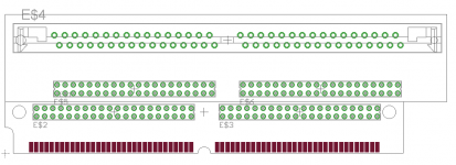
Thanks, tt, I can use that graphic! :approve:
From my perspective the Ultra ATA cable header rows will have to be moved up and away from the SIMM Mounting Tab Holes for clearance there, it looks like you've allowed for connector clearance already. I'll do a cardboard fit prototype to see if the clearances will out work with all the connectors in place. Did you confirm that the outboard ends of the IDE cables will not interfere with snapping in/keeping the SIMM in place?
As I said, I can easily be persuaded to do a Seed project if the price is right, but my way has several advantages.
I don't mind taking the time to do the grunt work of assembly from my normal manual process for layout/fab. Being a blast from the 1989 past, it'll be fun, relaxing and theraputic. The IDC ribbon cable mod and use makes for far less expensive multiple/differential length testing process, start long re-munch for successively shorter lengths. I'll probably start off with the nastiest connection first, three feet of standard, crosstalk inducing, non-alternating ground line ribbon cable, one in four odds on that one.
I give that a 50% chance of working reliably with a cable that places my IIsi SIMM in the space under the FDD. [ ] ]'>
] ]'>
I "know" the project is feasible, down, dirty, fugly, cheap as can be proof, with a side of DeclROM adapter board is almost impossible to resist, from my hacks development program perspective.
p.s. If someone else in the gang wants to adopt this line of research, sans the ROM adapter portion, to Seed the way for the rest of us, it IS a community project! [ ] ]'>
] ]'>
Besides, I can spend the extra money to replace my storage room whirlpooled Drill Press before I move in with my girlfriend. }
From my perspective the Ultra ATA cable header rows will have to be moved up and away from the SIMM Mounting Tab Holes for clearance there, it looks like you've allowed for connector clearance already. I'll do a cardboard fit prototype to see if the clearances will out work with all the connectors in place. Did you confirm that the outboard ends of the IDE cables will not interfere with snapping in/keeping the SIMM in place?
As I said, I can easily be persuaded to do a Seed project if the price is right, but my way has several advantages.
I don't mind taking the time to do the grunt work of assembly from my normal manual process for layout/fab. Being a blast from the 1989 past, it'll be fun, relaxing and theraputic. The IDC ribbon cable mod and use makes for far less expensive multiple/differential length testing process, start long re-munch for successively shorter lengths. I'll probably start off with the nastiest connection first, three feet of standard, crosstalk inducing, non-alternating ground line ribbon cable, one in four odds on that one.
I give that a 50% chance of working reliably with a cable that places my IIsi SIMM in the space under the FDD. [
] ]'>I "know" the project is feasible, down, dirty, fugly, cheap as can be proof, with a side of DeclROM adapter board is almost impossible to resist, from my hacks development program perspective.
p.s. If someone else in the gang wants to adopt this line of research, sans the ROM adapter portion, to Seed the way for the rest of us, it IS a community project! [
] ]'>Besides, I can spend the extra money to replace my storage room whirlpooled Drill Press before I move in with my girlfriend. }
Rob, that is so cool. Way to go. This is better entertainment than, well most things which are sold as entertainment. Although my son's 10 - 10 ball game last night was quite suspenseful. Some of the most entertaining baseball I've ever seen.
Although my son's 10 - 10 ball game last night was quite suspenseful. Some of the most entertaining baseball I've ever seen.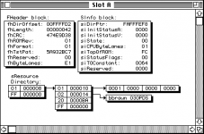
I've written a declrom validator that finds the byte lanes, checks the signature, pulls the length and crc, then computes the CRC. The CRC computation for my card was failing because out of the 66 bytes of my declrom, 2 bytes were being read back differently from what is stored on the 29F040. It helped me track down a mixup of A6 and A8, and once that was figured out, it worked.
I've found I can use either /STERM or /DSACK to acknowledge the read operation. /STERM is supposedly for synchronous operations and /DSACK is for asynchronous, and the 2 /DSACK signals allow for dynamic bus sizing vs. /STERM which is for 32bit bus. My application is a 32bit bus so the bus sizing isn't relevant, and I don't really understand the synchronous vs. asynchronous operation aspect, or if there's even a difference on the mac.
Right now, I'm using /DSACK{0,1}.
To recap:
A2-A20 from the PDS go straight to the 29F040's A0-A18D24-D31 from the PDS go to the 29F040's DQ0-DQ7.The 29F040's /CE is connected to GND, and /WE is connected to VCC.
The address decoding for access to 0xFAXXXXXX is done with:
A24 and A26 from the PDS get inverted by a 7404
/A24, /A26, A25, A27, A28-A31 all get ANDed by a 7408, and the result gets inverted by the 7404, and sent to /OEI know Dennis Nedry pointed out a way to do this with fewer gates, but this is what I did initially and it seems to work, so unless I need to rewire all that logic, I'd rather not.
The /OE line (in addition to being connected to the 29F040) is being sent to the C input of two 74125's, with the A input of each being connected to GND. The output of these two 74125's are being sent to /DSACK0 and /DSACK1.
I've also tried the same config with one 74125 gate and just using /STERM instead of /DSACK, and the results seem the same.
Now that it mostly works, I'll see if I can put this into Osmond PCB and experiment with that.
I guess I've made an 030 PDS card complete with firmware for use on a Mac. Neat. Too bad it doesn't actually do anything.
who cares if it doesnt do anything, its the point that the card is "seen" and can be "used" by the mac. So, next step is add a microcontroller to it or something so you can do stuffs with it.
Very nifty, that's awesome that you have it working! Nice work!
I'm wondering if there's any kind of timing requirement for the DSACK or STERM pins -- for example, is it only supposed to go low x nanoseconds after valid data has been placed onto the bus? I started looking in the 68030 manual but quickly lost interest, it's quite a monster. I'm just wondering if the scheme where /OE is going through the tristate buffers into the ack pins might technically be breaking timing requirements that could cause weird problems given the right set of circumstances, and if so, how to correct for that.
I'm wondering if there's any kind of timing requirement for the DSACK or STERM pins -- for example, is it only supposed to go low x nanoseconds after valid data has been placed onto the bus? I started looking in the 68030 manual but quickly lost interest, it's quite a monster. I'm just wondering if the scheme where /OE is going through the tristate buffers into the ack pins might technically be breaking timing requirements that could cause weird problems given the right set of circumstances, and if so, how to correct for that.
Yeah, this seems like quite a hack. I've looked at the timing diagram and can pretty much guarantee it's not doing the right thing. I can't say I really understand the process. This is also about the limit of my ability to work with all these wires on the protoboard though. I was going to see if I can put it onto a PCB as is, just to simplify any further hacking.
I just did it as a quick demo, showing much of the work is already completed with the libraries available in the program. No mechanical study or anything was done. I guess I tend to favor speed when working on projects since I feel the longer they go the less likely I will finish them. But if you don't mind soldering the connection points, then I say go for it with an etched board fabbed at home. Only thing I'm wondering is if the connectors would somehow make a difference with signal integrity. I think the SeedStudio price would be about $35 to make 10 4"x4" boards. The SIMM connector would have to hang off the edges of the board since it would go over 4" with the layout I posted earlier.
Yes!!! That is an awesome accomplishment, great work. :b&w:I guess I've made an 030 PDS card complete with firmware for use on a Mac. Neat. Too bad it doesn't actually do anything.
8-o My friend . . . saying that is akin to saying that dougg3 just managed to change the startup sound on his IIci . . . :lol:I guess I've made an 030 PDS card complete with firmware for use on a Mac. Neat. Too bad it doesn't actually do anything.
< . . . manages to hold his . . . tongue? . . . wanders to the fridge to make a root beer toast to this fabulous accomplishment . . . >
< . . . muttering: wire wrap . . . wire wrap . . . wire wrap under his breath the whole time . . . ;D >
I did some more googling and came upon this interesting document about interfacing through the SE/30 PDS to a National Semiconductor SONIC ethernet controller...
http://bitsavers.informatik.uni-stuttgart.de/pdf/national/_appNotes/AN-0691.pdf
Toward the end it provides a few basic boolean equations for some of the glue logic that handles activating the PROM and replying with the DSACK stuff. Looks like some of it is related to being a bus master, but I think there's enough in those equations to describe how the PROM should reply as a slave as well. It might be useful...looks pretty much the same as what you're doing except it also takes the address strobe pin into account.
http://bitsavers.informatik.uni-stuttgart.de/pdf/national/_appNotes/AN-0691.pdf
Toward the end it provides a few basic boolean equations for some of the glue logic that handles activating the PROM and replying with the DSACK stuff. Looks like some of it is related to being a bus master, but I think there's enough in those equations to describe how the PROM should reply as a slave as well. It might be useful...looks pretty much the same as what you're doing except it also takes the address strobe pin into account.
Ditto! P.S. the blank SIMMs and sockets are finally on the way to you...
Thanks! Yeah, /AS will be dropped before the address bits are, so it'll get /DSACK dropped earlier in the process like the timing diagrams. That's a good idea, thanks.
As I think about the possibility of adding more than just a flash chip to this, more address decoding becomes necessary. I'm enabling output for the 29F040 if anything in the slot is addressed, when it really should just be enabling if it's at the top of the address space. This seems easy enough with more 7408's, but it seems like it quickly gets out of hand. I'll play around with this in Osmond PCB, but like we were talking about, this is where an FPGA would be nice. An FPGA dev kit might be in my future.
As I think about the possibility of adding more than just a flash chip to this, more address decoding becomes necessary. I'm enabling output for the 29F040 if anything in the slot is addressed, when it really should just be enabling if it's at the top of the address space. This seems easy enough with more 7408's, but it seems like it quickly gets out of hand. I'll play around with this in Osmond PCB, but like we were talking about, this is where an FPGA would be nice. An FPGA dev kit might be in my future.
Yeah, an FPGA would greatly simplify making some of the logic stuff. You may only need a CPLD, depending on how complex the logic gets. CPLDs are nice because they typically have internal flash so they don't have to be externally loaded when they're powered up--many (most?) FPGAs need another flash chip attached. I do have a Lattice FPGA that doesn't need flash, but most others do from my understanding.
Also keep in mind you'll have to find 5V parts or do level shifting. Just like my RAM struggles, hopefully it isn't too hard to find 5V FPGAs or CPLDs or whatever...edit: looks like 5V CPLDs are still plentiful.
Also keep in mind you'll have to find 5V parts or do level shifting. Just like my RAM struggles, hopefully it isn't too hard to find 5V FPGAs or CPLDs or whatever...edit: looks like 5V CPLDs are still plentiful.
Since I'm dreaming, would it be possible to eventually make a cost-effective USB card with this? (>$50)
I honestly think the answer to that is "yes". Take an FPGA/CPLD, create some registers inside it that the Mac talks to over the PDS, then hook the CPLD/FPGA to a microcontroller with USB host capability. The microcontroller would talk to the CPLD/FPGA, do the USB work, and return data. Then get bbraun to write software for it. it would probably be slow, but it could be done that way (I think). Might take bus mastering capability to get faster speeds...
With the approach I'm thinking of, you'd have to target specific functionality--like storage or mouse or keyboard--rather than a generic USB stack on the Mac. I think the USB stack could be done too, but it would take a lot more effort...
Just my 2 cents!
it would probably be slow, but it could be done that way (I think). Might take bus mastering capability to get faster speeds...With the approach I'm thinking of, you'd have to target specific functionality--like storage or mouse or keyboard--rather than a generic USB stack on the Mac. I think the USB stack could be done too, but it would take a lot more effort...
Just my 2 cents!
I don't know anything about pricing, but as for functionality, anything is possible with sufficient time and resources right?
The steps I'm thinking of go something like this:
1) get what I have onto a PCB. I've not done any of this before, and figuring out PCB software is turning into a more challenging task than getting this working in the first place!
2) refine the bus interaction. I'd like to address the /STERM & /DSACK timing concerns, and I'd like to get the address decoding a little more refined. Specifically, only enabling the ROMs when addressing the end of the address space, and a bonus would be making the super slot space work too. This could be done with more discrete logic, CPLD, FPGA, etc.
3) investigate adding something more complex, like USB controller or similar. My thought process on this seems similar to dougg3's. At least initially, I'd plan on a general approach of the peripheral being "smart" and providing a "dumb" interface to the host processor. For instance, if we had a microprocessor with USB host or OTG support, have the microprocessor handle all the USB details, and for a USB disk just present a simple linear array of bytes to the Mac. Then the driver software is simple, and potentially much faster than having the host CPU execute a complex software stack.
4) explore the host processor side possibilities. We'll all have a much better idea on what is/isn't feasible as things take shape.
Anyway, baby steps. A week ago I didn't know what /STERM, /DSACK, or these tristate buffers were.
The steps I'm thinking of go something like this:
1) get what I have onto a PCB. I've not done any of this before, and figuring out PCB software is turning into a more challenging task than getting this working in the first place!
2) refine the bus interaction. I'd like to address the /STERM & /DSACK timing concerns, and I'd like to get the address decoding a little more refined. Specifically, only enabling the ROMs when addressing the end of the address space, and a bonus would be making the super slot space work too. This could be done with more discrete logic, CPLD, FPGA, etc.
3) investigate adding something more complex, like USB controller or similar. My thought process on this seems similar to dougg3's. At least initially, I'd plan on a general approach of the peripheral being "smart" and providing a "dumb" interface to the host processor. For instance, if we had a microprocessor with USB host or OTG support, have the microprocessor handle all the USB details, and for a USB disk just present a simple linear array of bytes to the Mac. Then the driver software is simple, and potentially much faster than having the host CPU execute a complex software stack.
4) explore the host processor side possibilities. We'll all have a much better idea on what is/isn't feasible as things take shape.
Anyway, baby steps. A week ago I didn't know what /STERM, /DSACK, or these tristate buffers were.
There off the shelf chips/MCUs with the entire USB architecture built in. Stack and all..
You would need a driver that enables the card to talk to the macintosh, and you need a secondary driver that enables USB Mass Storage, so once the USB device is put in, the driver of the card knows how to handle it.
I can handle PCB/CAD software. hehe. Footprints are a royal pain in the ass though.
Babysteps USB wise, would be start simpler. Use Serial, Slow Yes.... BUT...
if you can get an MCU that handles USB/USB Mass Storage and can interface the MCU through the serial port, you can write software/drivers to handle it. That will at least make sure you learned the USB MCU your using, and got all the software working.
Best thing would be to somehow patch the USB Mass Storage into the SCSI manager so formatting software like LIDO would see and format it. Otherwise youll have to write your own utility, and a driver that allows it to mount in finder.
I can/have made a simple app and an AVR that reads an SD card, prints its contents in the app, and gives me 512bytes in which sector/LBA that i request. The problem lies in the ability to take that, and make it into a driver that allows finder to use it. Something that I cannot do.
Which begs the question, How do you write a storage driver for macintosh?
You would need a driver that enables the card to talk to the macintosh, and you need a secondary driver that enables USB Mass Storage, so once the USB device is put in, the driver of the card knows how to handle it.
I can handle PCB/CAD software. hehe. Footprints are a royal pain in the ass though.
Babysteps USB wise, would be start simpler. Use Serial, Slow Yes.... BUT...
if you can get an MCU that handles USB/USB Mass Storage and can interface the MCU through the serial port, you can write software/drivers to handle it. That will at least make sure you learned the USB MCU your using, and got all the software working.
Best thing would be to somehow patch the USB Mass Storage into the SCSI manager so formatting software like LIDO would see and format it. Otherwise youll have to write your own utility, and a driver that allows it to mount in finder.
I can/have made a simple app and an AVR that reads an SD card, prints its contents in the app, and gives me 512bytes in which sector/LBA that i request. The problem lies in the ability to take that, and make it into a driver that allows finder to use it. Something that I cannot do.
Which begs the question, How do you write a storage driver for macintosh?
I've got what I think is the connector, the chips and the connections all into Osmond. I'm not sure I've got the orientation of the board correct. As in, the chips on the right side of the board when the card is installed into a machine.
Anyway, my files are all here. The 030Card.osm file is the project file and should be all that's needed. The others define parts, list of parts, and connections. Osmond is a free download, and works on OSX, so if anyone wants to take a look, feedback is appreciated.
U1-U4 are 29F040's
U5 is 7404
U6 and U7 are 7408's
U8 is 74125
I haven't figured out how (or if it's reasonable) to make something appear to the SCSIMgr. Everything I've done is more along the lines of the floppy & EDisk driver, that just present a "drive" to the OS, which is a linear array of 512byte blocks. When the "drive" structure is given to the OS, your driver is associated with it and the Prime routine will be called whenever a read or write operation is performed. The drive will show up in the Finder when a diskEvt event is posted using PostEvent. If the disk needs formatting, you'll get the "Uninitialized disk has been inserted, do you want to eject or initialize" dialog.
Icon retrieval and information about the size of the disk, whether it can be ejected, is read-only, etc. is handled by the driver's Control call.
Anyway, my files are all here. The 030Card.osm file is the project file and should be all that's needed. The others define parts, list of parts, and connections. Osmond is a free download, and works on OSX, so if anyone wants to take a look, feedback is appreciated.
U1-U4 are 29F040's
U5 is 7404
U6 and U7 are 7408's
U8 is 74125
Hook me up! I'll take a stab at it. Or if you'd like to do it yourself, the ROMDisk driver should be a fairly simple C based example using CodeWarrior 10. It's really just a lot of glue that boils down to a memory copy. The complications usually come in when the memory copy becomes something more complicated, like calling another driver, or something along those lines. I'd be glad to help out in any way.
I haven't figured out how (or if it's reasonable) to make something appear to the SCSIMgr. Everything I've done is more along the lines of the floppy & EDisk driver, that just present a "drive" to the OS, which is a linear array of 512byte blocks. When the "drive" structure is given to the OS, your driver is associated with it and the Prime routine will be called whenever a read or write operation is performed. The drive will show up in the Finder when a diskEvt event is posted using PostEvent. If the disk needs formatting, you'll get the "Uninitialized disk has been inserted, do you want to eject or initialize" dialog.
Icon retrieval and information about the size of the disk, whether it can be ejected, is read-only, etc. is handled by the driver's Control call.
I opened it in Osmond, but I just see the components laid-out, how do I get the traces to appear? (I tried importing the netlist.)
Well, that's the part I'm still trying to figure out. I haven't routed anything manually yet. AFAICT, Connect tool (the two arrows pointing at each other), and if you click on a pin, it will show the pin you clicked on in blue (if there's a connection defined), and all the other things it connects to in pink. If you option-click on a pin, it'll show a suggested trace, and then you use the other tools (to the right of the scissors) to move the trace around.
I'm still playing around with that part.
I'm still playing around with that part.
Interfacing to a USB mass storage device in a microcontroller supporting USB is really really simple, especially if you use a library like LUFA. In fact, the same chip I use on the SIMM programmer would be capable of it (except it would need to be the AT90USB647 rather than the 646 though, because the 646 only supports being a device). Another advantage of going the AVR route is the AVR can run at 5V. LUFA comes with tons of sample code demonstrating how to do it. It's the same library I've been using for the SIMM programmer.
Not pushing for any choice in particular, but I'm just saying that I agree with techknight -- it's way easy to do with a microcontroller that has USB built in. Making sample code to return 512-byte blocks from a USB drive would be a cinch.
Not pushing for any choice in particular, but I'm just saying that I agree with techknight -- it's way easy to do with a microcontroller that has USB built in. Making sample code to return 512-byte blocks from a USB drive would be a cinch.
p.40 already gang! :approve:
What are the response time differences between an SD Card, your typical Thumb Drive and SDRAM?
If we're going to lay storage out as memory acreage to parcel out for the CPU, why not use a relatively inexpensive SDRAM module as a battery backed Silicon Disk?
Heck, with Compact Virtual and the Killy Klip 68000 PDS hack we could be looking at a LOT of Virtual Memory and a hard disk replacement in an beige box compact Mac.
It'd be way cool in my IIsi and IIfx as well! }
What are the response time differences between an SD Card, your typical Thumb Drive and SDRAM?
If we're going to lay storage out as memory acreage to parcel out for the CPU, why not use a relatively inexpensive SDRAM module as a battery backed Silicon Disk?
Heck, with Compact Virtual and the Killy Klip 68000 PDS hack we could be looking at a LOT of Virtual Memory and a hard disk replacement in an beige box compact Mac.
It'd be way cool in my IIsi and IIfx as well! }
Got it...if I got to Design, "Make Rat's Nest" it shows the connections.
I'm looking at my Radius "SE30 Bus Adapter" and it has the 1-40 row numbers going the other direction, basically A1 in the top-right corner for the orientation of the board you posted. Not sure if this is an issue...