

Thread
Another IIci ROM hack
Yeah, that's what I'm concerned about. Maybe I made the part backwards?
I think so...it the notch/naming on the Radius board seems to agree with the GttMFH. Trash can check too, I think he has the same board.
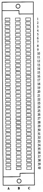
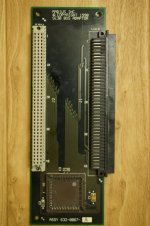
Ill go and dig through my files and try and find it. its been long ago, and i made it as a proof of concept precursor to making an MP3 player. (SD card, not USB).
But about the mac and C, Thats the whole thing. I dont program in C, and i know very little about it. Everything programming related that I have always done was in BASIC/Visual Basic.
I compile AVR Code in BASIC, the few mac apps i have written was in RealBASIC. I cant code C. hehe. Also the libraries I used for the SD card were part of the compiler I use, and uses the SPI of the SD card which is about as slow if not slower than the MAC Serial. LOL. But it was a proof of concept, and it did work.
i agree with Trash, not to say you would even use DDR2 ram, I have literally a bag, 66 sticks to be exact, of 512meg DDR2 533mhz ram.
my point is, ram disks are shot down because of cost, yeah a TB of ram is still rather pricy!, but were only talking about maybe 256mb to 512mb's would be plenty!
and sick fast! throw a 3.3v lithium battery on there just incase there is a power spike. USB wold be cool, popping in a 8gb sd card that costs only a few bucks, that can mirror ram by clicking on an icon, and then pooping that into any modern computer of your choice.
my point is, ram disks are shot down because of cost, yeah a TB of ram is still rather pricy!, but were only talking about maybe 256mb to 512mb's would be plenty!
and sick fast! throw a 3.3v lithium battery on there just incase there is a power spike. USB wold be cool, popping in a 8gb sd card that costs only a few bucks, that can mirror ram by clicking on an icon, and then pooping that into any modern computer of your choice.
To do routing, in most, if not all CAD software you need whats called a Netlist. This is the network persay, that ties the entire system together.
So you cant really draw a line from pin 1 of chip 1 to pin 2 of chip 2 unless you have a netlist that ties the 2 together to whats called a "ratline"
Every cad software is different, but the one I use is like this. Called FreePCB (which is free).
Where does the netlist come from? Well theres 2 ways. 1 you can build it manually. but, 2, it comes from the schematic. For example EAGLE. If you draw up a schematic and it has no errors, it will build a netlist and import it into the CAD router. This way you CANT make mistakes.
So you cant really draw a line from pin 1 of chip 1 to pin 2 of chip 2 unless you have a netlist that ties the 2 together to whats called a "ratline"
Every cad software is different, but the one I use is like this. Called FreePCB (which is free).
Where does the netlist come from? Well theres 2 ways. 1 you can build it manually. but, 2, it comes from the schematic. For example EAGLE. If you draw up a schematic and it has no errors, it will build a netlist and import it into the CAD router. This way you CANT make mistakes.
The easiest way for me to do a serial based mass-storage device with an SD card for starters, is having a MAC driver as you say to present a disk to finder with 512byte sectors.
But say if we can draft up a protocol quick-like, we can make this work.
For example a protocol that would do like this:
(Serial port)
Send a byte out the serial port to tell the external device that I request a read, or a write. So, $0A for read, $0B for Write (hypothetically).
So in this example, $0B for Write.
Receive ACK.
Send LBA Addy.
Recieve ACK.
Send 512bytes data + CRC.
Recieve Ack once complete. ACK here serves 2 purposes. 1, to let the driver know the data was received properly. 2, the external device is no longer busy processing the write. Driver wont get the Ack until the write is complete, 2 birds with 1 stone.
a NACK would indicate bad checksum/data and require driver to resend.
Then a check somewhere that if it fails too many times, report write error to OS.
Same thing comes with a read.
$0A for read
ACK
Send LBA
ACK + Data+ CRC
Driver checks validity and replies ACK/NACK to external device. NACK means the device will resend the data. Failure here too many times, report read error to OS.
Something like this, I can code microcontroller software to do. But i need the MAC software/driver/control panel to handle this. Now of course, this is dirt simple. about as simple as it gets. No provisiing for control such as maximum LBA size, etc... isnt provisioned here. this is simple read and write.
LBA size could be another command, like $0C.
$0C = Get Disk Capacity.
ACK + total blocks LBA + CRC
But say if we can draft up a protocol quick-like, we can make this work.
For example a protocol that would do like this:
(Serial port)
Send a byte out the serial port to tell the external device that I request a read, or a write. So, $0A for read, $0B for Write (hypothetically).
So in this example, $0B for Write.
Receive ACK.
Send LBA Addy.
Recieve ACK.
Send 512bytes data + CRC.
Recieve Ack once complete. ACK here serves 2 purposes. 1, to let the driver know the data was received properly. 2, the external device is no longer busy processing the write. Driver wont get the Ack until the write is complete, 2 birds with 1 stone.
a NACK would indicate bad checksum/data and require driver to resend.
Then a check somewhere that if it fails too many times, report write error to OS.
Same thing comes with a read.
$0A for read
ACK
Send LBA
ACK + Data+ CRC
Driver checks validity and replies ACK/NACK to external device. NACK means the device will resend the data. Failure here too many times, report read error to OS.
Something like this, I can code microcontroller software to do. But i need the MAC software/driver/control panel to handle this. Now of course, this is dirt simple. about as simple as it gets. No provisiing for control such as maximum LBA size, etc... isnt provisioned here. this is simple read and write.
LBA size could be another command, like $0C.
$0C = Get Disk Capacity.
ACK + total blocks LBA + CRC
Oh, and not to mention if we code this up, we could put it in ROM, no? then we could boot old machines off a serial based SD card reader. SLOW... YES... but it would work!. Besides im thinking Serial-SD card for sneakernet anyway. not for booting, or huge file transfers.
And once the protocol is finalized and in place, we could make the PDS card work, only difference being is that will run a parallel data operation instead of serial. Or you can just use a PIO chip that can interface to 030 and add a "third arbitary serial port" that only the driver knows about
My goal personal wise is to replace the modem card in my mac portable with an SD card reader and sneakernet things back and forth without floppies. Hell i could even throw a mux in there and toss a serial based WiFi card in there and have network at the same time as SD storage.
We kinda need a new thread for this as this is a whole different tangent. Oh well at least i might be on to something? But i could engineer the hardware and firmware to make this happen. But i would need someone such as bbraun and/or doug3 to write the mac driver to interface.
I laid out a simple protocol as a starting base, maybe someone can refine it or change it. either way. That could be the starting tree if we can iron out a solid protocol then driver to hardware interfacing would be simple. Just follow the protocol and everything would be ok :scrambled:
Edit: P.S. The device could be wireless too. In theory. Serial SPP modules are dirt cheap, and with that in mind if they are paired together, can create a serial wireless link. So in theory it could be wireless. This could be handy for localtalk. I have done this once with xBee but i dont like those modules that well, but with xBee modules they can work in broadcast mode so multiple machines can be on the same wireless channel and be on the same network. BT is point-to-point so that isnt an option.
And once the protocol is finalized and in place, we could make the PDS card work, only difference being is that will run a parallel data operation instead of serial. Or you can just use a PIO chip that can interface to 030 and add a "third arbitary serial port" that only the driver knows about
My goal personal wise is to replace the modem card in my mac portable with an SD card reader and sneakernet things back and forth without floppies. Hell i could even throw a mux in there and toss a serial based WiFi card in there and have network at the same time as SD storage.
We kinda need a new thread for this as this is a whole different tangent. Oh well at least i might be on to something? But i could engineer the hardware and firmware to make this happen. But i would need someone such as bbraun and/or doug3 to write the mac driver to interface.
I laid out a simple protocol as a starting base, maybe someone can refine it or change it. either way. That could be the starting tree if we can iron out a solid protocol then driver to hardware interfacing would be simple. Just follow the protocol and everything would be ok :scrambled:
Edit: P.S. The device could be wireless too. In theory. Serial SPP modules are dirt cheap, and with that in mind if they are paired together, can create a serial wireless link. So in theory it could be wireless. This could be handy for localtalk. I have done this once with xBee but i dont like those modules that well, but with xBee modules they can work in broadcast mode so multiple machines can be on the same wireless channel and be on the same network. BT is point-to-point so that isnt an option.
tt: Thanks for catching that, I think I've corrected the orientation. I've updated the project file with the renumbering change.
techknight: sounds good. I've sent you some protocol feedback, and for a serial device I can get started by doing some serial comms against a modern machine just to test it out and get a jump start before having hardware.
techknight: sounds good. I've sent you some protocol feedback, and for a serial device I can get started by doing some serial comms against a modern machine just to test it out and get a jump start before having hardware.
Sooo cool. I wish I had time to participate.
Remember, when using Osmond (or any PCB software) to pay attention to whether you're seeing a view of the layer or a view through the board to the "back" of the layer. I laid out an 8 pin SOIC mirrored on my first board because of that.
Here's a little old discussion about SCSI Mgr, which might be interesting. It's too bad that "Driverguru" just dropped in for a few days and then went away again. Still, if you get to where you need some specific questions addressed, it might be worth trying to track him down:
http://68kmla.org/forums/viewtopic.php?p=61401#p61401
I had always thought it terms of interfacing a USB chip directly to the Mac's bus, but the idea of using a microcontroller as a DMA/driver engine for the USB controller is great.
Still, I think it might be worth taking a look at the USB chip I referenced up thread. I didn't read the whole datasheet, but it said something about an on-board microcontroller in the introductory blurb. With the configurable I/O pins, one might not even need any programmable logic to interface it. And it says it has 5V safe inputs. If that really means what it says, level shifters should be unnecessary.
http://www.ftdichip.com/Support/Documents/DataSheets/ICs/DS_Vinculum-II.pdf
This one is available at DigiKey in the 64 pin QFP for ~$6.
Edit: Bah! Never mind on the above chip. It has a really nifty 40 pin GPIO mode which could probably be made to interface with the 68030 bus without any glue, but while it is "USB 2.0 compliant" it does not support 480 Mbps (High Speed) because "the power requirements are deemed excessive for VNC2 target applications."
Double Bah!
Remember, when using Osmond (or any PCB software) to pay attention to whether you're seeing a view of the layer or a view through the board to the "back" of the layer. I laid out an 8 pin SOIC mirrored on my first board because of that.
Here's a little old discussion about SCSI Mgr, which might be interesting. It's too bad that "Driverguru" just dropped in for a few days and then went away again. Still, if you get to where you need some specific questions addressed, it might be worth trying to track him down:
http://68kmla.org/forums/viewtopic.php?p=61401#p61401
I had always thought it terms of interfacing a USB chip directly to the Mac's bus, but the idea of using a microcontroller as a DMA/driver engine for the USB controller is great.
Still, I think it might be worth taking a look at the USB chip I referenced up thread. I didn't read the whole datasheet, but it said something about an on-board microcontroller in the introductory blurb. With the configurable I/O pins, one might not even need any programmable logic to interface it. And it says it has 5V safe inputs. If that really means what it says, level shifters should be unnecessary.
http://www.ftdichip.com/Support/Documents/DataSheets/ICs/DS_Vinculum-II.pdf
This one is available at DigiKey in the 64 pin QFP for ~$6.
Edit: Bah! Never mind on the above chip. It has a really nifty 40 pin GPIO mode which could probably be made to interface with the 68030 bus without any glue, but while it is "USB 2.0 compliant" it does not support 480 Mbps (High Speed) because "the power requirements are deemed excessive for VNC2 target applications."
Double Bah!
Cool...It looks consistent with my artifacts.
But....you forgot to include the right-angle pass-through connector on the other side.
 ) But now I'm reminded of a question I've had, is the PDS slot completely parallel if you want to add more slots say for a dummy adapter that Trash has brought up?
Thanks. Passthrough is beyond my routing abilities at the moment. In fact, I've routed 7 traces in 3 hours and needed 4 layers to do it. How many layers can I have? I'm thinking I'll probably need 40-60 layers.
Yeah, I was J/K, that would add many more lines to route. I would try to get it in 2-layers otherwise the fab cost is much higher. Then in general the options seem to jump from 2 to 4 layers for protos.
Maybe the traces you are using are too wide? This shot shows you can fit two traces in between each pin: viewtopic.php?f=29&t=19369#p183281 Also, you can use vias to jump sides of the board if you need to cross-over a trace.
Maybe the traces you are using are too wide? This shot shows you can fit two traces in between each pin: viewtopic.php?f=29&t=19369#p183281 Also, you can use vias to jump sides of the board if you need to cross-over a trace.
Actually, mine's the DayStar Adapter with provision for adding Zeners to damp over-voltages on the signals.

Come to think of it, these cards would be perfect as a Prototyping Riser/Chassis for playing with the PDS in your open topped IIsi, bb, or on your bare MoBo SE/30 testing config, tt. I'll bet macmetex still has at least half a bucket full and the price is right.
Just de-solder the RA PassThru Connector and solder headers onto the back side of the board, then solder a prototyping board directly onto the headers and you're good to go. Add the Zener Diodes if noise becomes problematic.
You can now wire wrap directly from the headers to wire wrap sockets for the ICs. Heck, the first Mac Mobo was made in wire wrap . . .
. . . as were the first two PC Prototypes. PaleoTech ROCKS! :approve:
Haha. You're funny. No seriously, if all I get are 4 layers, I may as well stop now.
Well, let's see what you have... I am playing around a little bit with it. BTW, do you know how to swap routed traces to another layer in Osmond?
You must be looking at PCB layout the way I do, like a graphic that makes sense in your head. Doin' it for real requires calming your mind, letting go of your beliefs and expectations . . . trust the force.
IOW, do the rat's nest thing and let the software worry about the routing, that's where application of the force comes into play. Wielding the force like a Paduan Learner ends up with too many required layers as well. By using just Apprentice level Jedi finesse earlier in the thread, dougg3 managed to pull out of an autoroutation death spin by manually placing a few, key, guide path inducing traces before using the force.
A real PCB guy is a Jedi in his application of the force. A Master PCB guy plays Jedi Mind games likely to make Master Yoda's head spin.
) edit: we're back up to p.40 again after being there temporarily . . . what's up with that? :?:
I don't know what's going on with needing so many layers, but I have a couple of suggestions.
First, use the tutorial. I think you did already, but just in case you skipped the bits on routing....
Second, read the specifications for the PCB service you hope to use and set your trace width and trace spacing to match. I believe that Seed Studio allows down 6 mil (6/1000") traces. Signal traces do not need to be any wider than that.
Third, keep the annular rings around your vias small. You can probably make them about 10 mils, (20 mils wider total than the via drill hole) and be okay, although I remember reading some handy guidelines somewhere once.
Fourth, this is more a matter of style, but if you're not using a netlist, first choose your PCB size. Then put your components on the board, generally where you expect them to land. Then use the (connection?) tool to connect the various pins which will connect together. Now you have a rats nest.
Now start routing the traces. When you need to add a via, you'll want to create the via in place, then use one of the tool (forget which one) to connect the via to the rats nest trace. Then cut the trace between one of the pins and the via. The pin should change colors because the netlist still says it should be connected, but it isn't any more. Then switch active layers of the board, and connect the pin and via back up on the other layer. If the pin doesn't exist on both layers, you'll need a second via, of course.
At least that's the way I remember doing it.
Fifth, try to use one layer for horizontal traces and the other layer for vertical traces. Switch between them with vias. This is not a firm rule -- it's down right floppy, but it's a useful state of mind.
Here's a two layer board I laid out. There are something like 300 pins on both connectors and I put it on 2 layers:
Both:

Front:

Back:

And here's the resulting board:

Didn't work though. That's a two layer board trying to act as a 40 - 50 MHz CPU adapter for the ANS. One of these days, I'll get back to it...
The JPGs are kind of low res. If you like I can upload the Osmond file when I get home tonight. It's about twelve years old, so I'm not certain that the file format is still compatible.
Actually, come to think of it, I have 50 or 60 saved files for this one design, if it hasn't been lost in the hard drive catastrophes over the years. Fifty or 60 saved files, because when I'm laying out circuit board I save often, and always do Save As, so I can revert to an earlier design.
So, my collection of saved files really is a record of the progression of the layout. Would that be helpful?
First, use the tutorial. I think you did already, but just in case you skipped the bits on routing....
Second, read the specifications for the PCB service you hope to use and set your trace width and trace spacing to match. I believe that Seed Studio allows down 6 mil (6/1000") traces. Signal traces do not need to be any wider than that.
Third, keep the annular rings around your vias small. You can probably make them about 10 mils, (20 mils wider total than the via drill hole) and be okay, although I remember reading some handy guidelines somewhere once.
Fourth, this is more a matter of style, but if you're not using a netlist, first choose your PCB size. Then put your components on the board, generally where you expect them to land. Then use the (connection?) tool to connect the various pins which will connect together. Now you have a rats nest.
Now start routing the traces. When you need to add a via, you'll want to create the via in place, then use one of the tool (forget which one) to connect the via to the rats nest trace. Then cut the trace between one of the pins and the via. The pin should change colors because the netlist still says it should be connected, but it isn't any more. Then switch active layers of the board, and connect the pin and via back up on the other layer. If the pin doesn't exist on both layers, you'll need a second via, of course.
At least that's the way I remember doing it.
Fifth, try to use one layer for horizontal traces and the other layer for vertical traces. Switch between them with vias. This is not a firm rule -- it's down right floppy, but it's a useful state of mind.
Here's a two layer board I laid out. There are something like 300 pins on both connectors and I put it on 2 layers:
Both:
Front:
Back:
And here's the resulting board:
Didn't work though. That's a two layer board trying to act as a 40 - 50 MHz CPU adapter for the ANS. One of these days, I'll get back to it...
The JPGs are kind of low res. If you like I can upload the Osmond file when I get home tonight. It's about twelve years old, so I'm not certain that the file format is still compatible.
Actually, come to think of it, I have 50 or 60 saved files for this one design, if it hasn't been lost in the hard drive catastrophes over the years. Fifty or 60 saved files, because when I'm laying out circuit board I save often, and always do Save As, so I can revert to an earlier design.
So, my collection of saved files really is a record of the progression of the layout. Would that be helpful?
I never had much luck with autorouting, usually it makes a big mess of things and needs a lot of manual cleanup and optimization so you don't end up with 5-10 vias on a single trace, noisy traces running through sensitive analog areas, etc. I manually route all my PCBs, it's an art, it takes time and patience, but the result IMHO is worth it.
Looks like it could use a pirate. I'm pretty sure it makes it faster. )
)
This is just a really rough stab at the lower end of the board with 2 layers. You might need to jumper some connections with wires in the worst case scenario. The upper area gets hairy... I think the chip spacing needs adjustment, I move some of the smaller ones down. I cheated with the vias and swapping layers, so some places might show an overlap, but the idea is there. It has been years since I laid-out a PCB in Eagle, but it seemed way easier to move components and swap layers while routing.
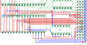
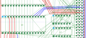
The vertical traces on the left side of U1 should probably be blue....it's an iterative process...
The vertical traces on the left side of U1 should probably be blue....it's an iterative process...
Wow, that's amazing tt. I was wondering if changing orientations of the chips would help, but from your pictures, it seems like that isn't necessary. Thanks a bunch for taking a look at this, what you got done in less than an hour... I'm not sure I'd have figured that out in weeks of staring at this.
FWIW, on the many boards I've inspected a/o collected, the ICs for I/O/Glue are normally parallel to the expansion slot connector. Memory buses can run either direction, but the ICs are perpendicular to the board connector, with the buses parallel to it, for most high capacity designs I've seen.
Remember, these are only casual observations on my part. :beige:
p.s. your care package arrived today, DQ!. That was fast!!!!!!!!!! USPS must have sensed the color of the boards . . .
. . . and the three Buccaneers on Board! :rambo:
Remember, these are only casual observations on my part. :beige:
p.s. your care package arrived today, DQ!. That was fast!!!!!!!!!! USPS must have sensed the color of the boards . . .
. . . and the three Buccaneers on Board! :rambo:
Well . . .
I've got so many projects on the table today I just didn't know which one on which to procrastinate first:
So, I looked over the ROM SIMM connectors, rummaged through the prototyping parts drawers and came up with a couple of really nasty, interesting ways to go about this extender test rig . . . and then spotted drawer with the 64 position machine pin headers. One . . . two . . . saw'em both in two and now I've got four 16 pin socket/pin row sets. Three . . . and those four are now all seated firmly upon the soldertail pin rows on one of the three connectors . . .
. . . but it's the boring, repetitive, least interesting way to go about this kluge.
. . . we got your good news: looked around a little more and found my bag of single row square header pin strips . . . all set.
. . . we got your bad news: the dang wire wrap tool is MIA!!!!!!!
. . . we got your obligatory silly question: will wire wrap even work on the round machine pins? Maybe just well enough to solder them in place?
Now it's procrastination time. :
Edit: picture of . . . progress?
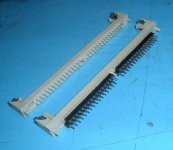
Wire wrap tool is still MIA.
I've got so many projects on the table today I just didn't know which one on which to procrastinate first:
So, I looked over the ROM SIMM connectors, rummaged through the prototyping parts drawers and came up with a couple of really nasty, interesting ways to go about this extender test rig . . . and then spotted drawer with the 64 position machine pin headers. One . . . two . . . saw'em both in two and now I've got four 16 pin socket/pin row sets. Three . . . and those four are now all seated firmly upon the soldertail pin rows on one of the three connectors . . .
. . . but it's the boring, repetitive, least interesting way to go about this kluge.
. . . we got your good news: looked around a little more and found my bag of single row square header pin strips . . . all set.
. . . we got your bad news: the dang wire wrap tool is MIA!!!!!!!
. . . we got your obligatory silly question: will wire wrap even work on the round machine pins? Maybe just well enough to solder them in place?
Now it's procrastination time. :
Edit: picture of . . . progress?
Wire wrap tool is still MIA.
Thanks, I hope it gives you some ideas, there's stuff I think could be better, but it is sort of a conceptual layout to see if 2 layers is feasible. Hopefully the design rules are not violated with the routing between pads. I can look at the upper part more sometime later, I am a little tied-up at the moment. But my approach is to look at general groupings of paths in the rat's nest and then see if they can be out of the way of the other groups. I see the upper right as having a bunch of intersections that will probably need a ton of vias unless a change in the chip layout could mitigate that issue. I am feeling constrained by the software, so I need to learn how to use it better within its workflow.
Note for later: Do you have the board size maxed out? If not, I would make it the max size for the board-house price point and fill the leftover area with a bunch of plated holes at 0.1" spacing for soldering other stuff later.
We ruled out ROM SIMM hacking the quadras because of a lack of slot info, right?
There are a lot of quadras.
The 700/900 works and has a SIMM slot from the factory.
My centris 610 came with a SIMM slot from the factory, and the ROM SIMM worked with it. Which probably means the Q610, 650, and 800, which don't come with a SIMM slot from the factory but do have solder pads, probably work as well. If you installed a SIMM slot.
Doug's research on the AV macs shows the current SIMM is incompatible with those (also no slot from the factory, you'd have to install one).
I don't think anyone has checked out the 630.
That's the hardware side. The software side has been focused on the IIsi ROM, which works for the IIsi and earlier (IIci, IIcx, IIx, SE/30), but won't work for newer machines. If there's sufficient interest, working on the newer ROMs is always a possibility. The 8MB SIMM opened up a lot of possibilities with newer ROMs that weren't really practical with the 2MB SIMM.
The 700/900 works and has a SIMM slot from the factory.
My centris 610 came with a SIMM slot from the factory, and the ROM SIMM worked with it. Which probably means the Q610, 650, and 800, which don't come with a SIMM slot from the factory but do have solder pads, probably work as well. If you installed a SIMM slot.
Doug's research on the AV macs shows the current SIMM is incompatible with those (also no slot from the factory, you'd have to install one).
I don't think anyone has checked out the 630.
That's the hardware side. The software side has been focused on the IIsi ROM, which works for the IIsi and earlier (IIci, IIcx, IIx, SE/30), but won't work for newer machines. If there's sufficient interest, working on the newer ROMs is always a possibility. The 8MB SIMM opened up a lot of possibilities with newer ROMs that weren't really practical with the 2MB SIMM.
i love the 8mb simm!
bbraun i also and very grateful for your hardwork sir!
also i would like to mention something,
Hey, bbraun, did you install a sound clip easter egg that randomly plays
a guy playing a video game, and saying i love this game ?
haha
bbraun i also and very grateful for your hardwork sir!
also i would like to mention something,
Hey, bbraun, did you install a sound clip easter egg that randomly plays
a guy playing a video game, and saying i love this game ?
haha
I know this is kind of off-topic to the latest development stuff, but I've been thinking and I just want to get this written down for future reference:
If I ever want to create a better, faster version of the SIMM programmer, this Atmel AVR32 chip seems like a good possibility:
AT32UC3C164C
66 MHz, USB support, works with 5V supply, has 81 I/O pins, 64 KB flash, 16 KB RAM, costs less than $10. That right there more than satisfies all of the requirements of the SIMM programmer. By eliminating the SPI GPIO extender and replacing it with a single processor with tons of pins, I'm pretty sure this thing could flash a SIMM *much* faster than is currently possible.
I recently ordered 50 of my current SIMM programmer PCBs, so I don't expect to make a new programmer anytime soon...but this is a possibility for the future! Or if anyone else gets brave and feels like designing something using this...
If I ever want to create a better, faster version of the SIMM programmer, this Atmel AVR32 chip seems like a good possibility:
AT32UC3C164C
66 MHz, USB support, works with 5V supply, has 81 I/O pins, 64 KB flash, 16 KB RAM, costs less than $10. That right there more than satisfies all of the requirements of the SIMM programmer. By eliminating the SPI GPIO extender and replacing it with a single processor with tons of pins, I'm pretty sure this thing could flash a SIMM *much* faster than is currently possible.
I recently ordered 50 of my current SIMM programmer PCBs, so I don't expect to make a new programmer anytime soon...but this is a possibility for the future! Or if anyone else gets brave and feels like designing something using this...
The final 8 MB SIMM PCBs have been ordered. 50 of them. I hope I didn't screw anything up!
They will be black, Jolly Roger centered on the back, no LEDs or anything. I left the hole in the Jolly Roger...I think it's fine. There will be vias going through it so it will be interesting to see how it turns out.
They will be black, Jolly Roger centered on the back, no LEDs or anything. I left the hole in the Jolly Roger...I think it's fine. There will be vias going through it so it will be interesting to see how it turns out.