

Thread
Another IIci ROM hack
Nope, he's talking about two layouts for SMT ROMs . . . IIRC, DIP ROMs don't exist in the capacities required . . . [ ] ]'>
] ]'>
. . . two ICs on each side = easier hand soldering of at least one side . . .
. . . four ICs on the same side = DIY SMT Component Installation (Toaster Oven Method) . . .
Two different activation temperature solder pastes = two step/two sided IC Baking! }
Methinks a new ROM Card Design is simmering in the Post Processing Lobes of several comrade's brains ATM! )
)
] ]'>. . . two ICs on each side = easier hand soldering of at least one side . . .
. . . four ICs on the same side = DIY SMT Component Installation (Toaster Oven Method) . . .
Two different activation temperature solder pastes = two step/two sided IC Baking! }
Methinks a new ROM Card Design is simmering in the Post Processing Lobes of several comrade's brains ATM!
)
Wow. Lots of discussion on the ROM module idea.
Yes, I have a ROM module laid out. I haven't looked at the design in a couple of years though so there could be some issues:
1) There might be a few details left to fix.
2) I may have it on an 8" X 10" panel with a bunch of IIfx SIMMs.
3) I had a hard drive failure a while back which wiped out a bunch of rocket engine press-form designs. I thought that I always made backups of my designs, but if those are gone, some of my circuit boards could be gone. I need to check this.
However, none of those is much of a problem. It doesn't take very long for me to lay one of these out. I am helped on the ROM layout by the fact that the SIMM socket is the same (IIRC) as the IIfx RAM SIMM. So I already have a part created for the edge connector size and pins and latch holes on the edges. And I know that this part works, because my IIfx SIMMs work.
Yes, the 63 mil vs 47 - 50 mil is the biggest problem. In fact, it bit both Gamba and I. We were working merrily along each doing our part to make that SIMM and Gamba emails me to say he finished the assembly and he can't get it into the ROM socket. At that point it had pins on both sides of the board.
So he filed/ground down the back side of the SIMM until the edge connector was .5" instead of .063". This works because it's a SIMM and not a DIMM.
And yes, one of the biggest things holding me back was that all the cheap circuit board fabrication options I could find were for "standard" .063" board.
So I was looking at having 100 - 200 of the board made and then I could populate them as needed. However, at the time that I actively looked at that, the price would have been ~$600 for the lot and the chances that there wouldn't be enough people who want one to pay back the cost seemed high.
Enter SeeedStudio, as bigmessofwires just presented. I've seen their offer before and it looks great:
http://68kmla.org/forums/viewtopic.php?p=148796#p148796
I just hadn't considered it in connection with the Mac II family ROM project. Thank you bigmessofwires. That should make it doable.
An academic issue, but perhaps of interest is that regular board fabrication has fallen in price a bit, or at least there are more special offers available. I think that having a hundred boards made, might cost more like $200 these days, because 4pcb.com keeps offering board specials with no NRE costs.
On a small run like this the NRE (non-recurring expenses) is what really kills a project.
As T80 surmises, I am discussing two different surface mount designs. There are through hole PLCC32 sockets. So it could be a through-hole design. However, if one made it through-hole, that would preclude soldering the chips directly to the board. For folks who just want a 32-bit clean ROM for their SE/30, chips soldered to the board is preferred.
On the other hand, surface mount PLCC32 sockets are a pain. If sockets are the goal, it's nicer to do through-hole.
On the gripping hand, surface mount PLCC32 sockets would be easier than through-hole if I was doing toaster oven soldering. But I'm not doing that yet. It's a dream. Maybe even a goal. But it's not on the horizon.
I suppose I could lay it out as surface mount pads with holes drilled in the middle where through hole could be mounted. I'm not certain, but I think the foot prints may be compatible.
What do people want? Hand assembly? Toaster assembly? Sockets only? Hybrid surface mount/through-hole layout?
Is there someone else who could do the assembly if I designed the boards?
And is there anyone else who is gung-ho to lay their design out immediately? It will take me some weeks, possibly months to get to this. I still need to finish the PEx ROM before I do anything else...
So, I'm willing to work on this. But I'm also willing to step aside if others can get to it faster.
Oh, and T80, very cool about the two temperature activation for the solder. One could always use leaded and lead-free solder. They have about a 20 - 30C difference in melting point. But one would need a good controller on the oven. I found a link a while back that pointed at some controllers for a little under $100. I was going to whip one up out of a microcontroller and SCR, but when it's all said and done, buying an existing product for $100 is probably cheaper than developing one's own solution, even if it looks like the DIY should be cheaper. Experience says it won't be...
Edit: T80, I just noticed that I missed your question about home-made vs. fabrication. In recent years all my thought has gone to commercial fabrication. For a while there I was going to do home-made. I was going to use the toner-transfer method:
http://www.pulsarprofx.com/
but ultimately decided it was too much trouble.
That's why I had the ROM SIMM laid out on an 8" X 10" panel with IIfx SIMMs (and some 30 pin SIMMs, IIRC). The toner transfer paper lends itself to doing 8.5" X 11" panels, or slightly smaller. I found some .050" double sided copper clad board in about those dimensions.
Making the boards sounds easy. Here's where it gets to be too much trouble: Vias.
One is left having to hand drill all the vias and then solder a wire through the board and onto each side. Alternatively, one could build a CNC-type drill (one fellow built one out of an old plotter). Once the holes are drilled, and before the board is etched, one could squeegee electrically conductive ink onto the board and then blow it through the holes, so that it coats the inside surface of each drilled hole. Then drop the whole board in a copper sulfate tank and electroplate until the ink-covered holes are coated in copper.
Setting up to electroplate is a pain. That conductive ink is either hard to find, or ridiculously expensive.
By the time I looked at all the problems that vias were going to cause, I decided it was better to just go with commercial fabrication.
If I had a workshop, where I could set up a permanent etch tank, and electroplating tank and associated stuff, then maybe....
And then there's solder mask. It's not strictly necessary, but it certainly reduces errors when assembling (soldering) the boards. It's a photosensitive laminate. Well, I already have a laminator to make the toner transfer method efficient, but then one needs a photo-exposer thingy to get the solder mask pattern onto the solder mask laminate. And at that point, one may as well abandon the toner transfer method and go to a full-on photo-resist method of etching the boards.
But again, the vias are a pain.
So, commercial fabrication all the way. There's a point at which one's volume is large enough to make it cheaper to buy/build all the stuff to do it at home, and I think that point is where one goes into business as a PCB fabrication house.
Yes, I have a ROM module laid out. I haven't looked at the design in a couple of years though so there could be some issues:
1) There might be a few details left to fix.
2) I may have it on an 8" X 10" panel with a bunch of IIfx SIMMs.
3) I had a hard drive failure a while back which wiped out a bunch of rocket engine press-form designs. I thought that I always made backups of my designs, but if those are gone, some of my circuit boards could be gone. I need to check this.
However, none of those is much of a problem. It doesn't take very long for me to lay one of these out. I am helped on the ROM layout by the fact that the SIMM socket is the same (IIRC) as the IIfx RAM SIMM. So I already have a part created for the edge connector size and pins and latch holes on the edges. And I know that this part works, because my IIfx SIMMs work.
Yes, the 63 mil vs 47 - 50 mil is the biggest problem. In fact, it bit both Gamba and I. We were working merrily along each doing our part to make that SIMM and Gamba emails me to say he finished the assembly and he can't get it into the ROM socket. At that point it had pins on both sides of the board.
So he filed/ground down the back side of the SIMM until the edge connector was .5" instead of .063". This works because it's a SIMM and not a DIMM.
And yes, one of the biggest things holding me back was that all the cheap circuit board fabrication options I could find were for "standard" .063" board.
So I was looking at having 100 - 200 of the board made and then I could populate them as needed. However, at the time that I actively looked at that, the price would have been ~$600 for the lot and the chances that there wouldn't be enough people who want one to pay back the cost seemed high.
Enter SeeedStudio, as bigmessofwires just presented. I've seen their offer before and it looks great:
http://68kmla.org/forums/viewtopic.php?p=148796#p148796
I just hadn't considered it in connection with the Mac II family ROM project. Thank you bigmessofwires. That should make it doable.
An academic issue, but perhaps of interest is that regular board fabrication has fallen in price a bit, or at least there are more special offers available. I think that having a hundred boards made, might cost more like $200 these days, because 4pcb.com keeps offering board specials with no NRE costs.
On a small run like this the NRE (non-recurring expenses) is what really kills a project.
As T80 surmises, I am discussing two different surface mount designs. There are through hole PLCC32 sockets. So it could be a through-hole design. However, if one made it through-hole, that would preclude soldering the chips directly to the board. For folks who just want a 32-bit clean ROM for their SE/30, chips soldered to the board is preferred.
On the other hand, surface mount PLCC32 sockets are a pain. If sockets are the goal, it's nicer to do through-hole.
On the gripping hand, surface mount PLCC32 sockets would be easier than through-hole if I was doing toaster oven soldering. But I'm not doing that yet. It's a dream. Maybe even a goal. But it's not on the horizon.
I suppose I could lay it out as surface mount pads with holes drilled in the middle where through hole could be mounted. I'm not certain, but I think the foot prints may be compatible.
What do people want? Hand assembly? Toaster assembly? Sockets only? Hybrid surface mount/through-hole layout?
Is there someone else who could do the assembly if I designed the boards?
And is there anyone else who is gung-ho to lay their design out immediately? It will take me some weeks, possibly months to get to this. I still need to finish the PEx ROM before I do anything else...
So, I'm willing to work on this. But I'm also willing to step aside if others can get to it faster.
Oh, and T80, very cool about the two temperature activation for the solder. One could always use leaded and lead-free solder. They have about a 20 - 30C difference in melting point. But one would need a good controller on the oven. I found a link a while back that pointed at some controllers for a little under $100. I was going to whip one up out of a microcontroller and SCR, but when it's all said and done, buying an existing product for $100 is probably cheaper than developing one's own solution, even if it looks like the DIY should be cheaper. Experience says it won't be...
Edit: T80, I just noticed that I missed your question about home-made vs. fabrication. In recent years all my thought has gone to commercial fabrication. For a while there I was going to do home-made. I was going to use the toner-transfer method:
http://www.pulsarprofx.com/
but ultimately decided it was too much trouble.
That's why I had the ROM SIMM laid out on an 8" X 10" panel with IIfx SIMMs (and some 30 pin SIMMs, IIRC). The toner transfer paper lends itself to doing 8.5" X 11" panels, or slightly smaller. I found some .050" double sided copper clad board in about those dimensions.
Making the boards sounds easy. Here's where it gets to be too much trouble: Vias.
One is left having to hand drill all the vias and then solder a wire through the board and onto each side. Alternatively, one could build a CNC-type drill (one fellow built one out of an old plotter). Once the holes are drilled, and before the board is etched, one could squeegee electrically conductive ink onto the board and then blow it through the holes, so that it coats the inside surface of each drilled hole. Then drop the whole board in a copper sulfate tank and electroplate until the ink-covered holes are coated in copper.
Setting up to electroplate is a pain. That conductive ink is either hard to find, or ridiculously expensive.
By the time I looked at all the problems that vias were going to cause, I decided it was better to just go with commercial fabrication.
If I had a workshop, where I could set up a permanent etch tank, and electroplating tank and associated stuff, then maybe....
And then there's solder mask. It's not strictly necessary, but it certainly reduces errors when assembling (soldering) the boards. It's a photosensitive laminate. Well, I already have a laminator to make the toner transfer method efficient, but then one needs a photo-exposer thingy to get the solder mask pattern onto the solder mask laminate. And at that point, one may as well abandon the toner transfer method and go to a full-on photo-resist method of etching the boards.
But again, the vias are a pain.
So, commercial fabrication all the way. There's a point at which one's volume is large enough to make it cheaper to buy/build all the stuff to do it at home, and I think that point is where one goes into business as a PCB fabrication house.
:lol: THX, trag! :b&w: Workarounds for the "it can't be done" problem set were my "stock in trade" back in the Sign Business and the Font Cartridge ( 4 x 32k ROMs) Emulator Startup day! [] ]'>
As for the thickness issue, NoPro! :approve: Just do the SIMM Layout WITHOUT the pads on the back side!
A makeshift router-table/sliding-table jig will handily solve that problem for ProtoPCBs a/o Production PCBs! [ ] ]'>
] ]'>
p.s. I'm best know as either Trash or jt (lower case) over on 'fritter and around these here parts!)
p.p.s. i see we're posting at the same time! True, Plated thru-holes are a major pain, but if you maximize the design for minimizing the Via count, things can work out great. I make the resists for double sided Proto-PCBs on the Vinyl Cutting Plotter, weed the high-performance sign vinyl VERY carefully, especially those little thru-hole centers for drill pressin' and just use a regular photo tray and CrapShack etchant.
One trick I came up with was to lay out all the signals so their side of the zener pads connected to traces through the board w/the other sides connected to common ground, which makes for a nice, quiet board! If you're doing the Toaster Oven Method, just sew up your board with bare copper wire and clip after soldering the other side . . .
. . . or do the SMT-2-Step and clip afterward! }
] ]'>As for the thickness issue, NoPro! :approve: Just do the SIMM Layout WITHOUT the pads on the back side!
A makeshift router-table/sliding-table jig will handily solve that problem for ProtoPCBs a/o Production PCBs! [
] ]'>p.s. I'm best know as either Trash or jt (lower case) over on 'fritter and around these here parts!
) p.p.s. i see we're posting at the same time! True, Plated thru-holes are a major pain, but if you maximize the design for minimizing the Via count, things can work out great. I make the resists for double sided Proto-PCBs on the Vinyl Cutting Plotter, weed the high-performance sign vinyl VERY carefully, especially those little thru-hole centers for drill pressin' and just use a regular photo tray and CrapShack etchant.
One trick I came up with was to lay out all the signals so their side of the zener pads connected to traces through the board w/the other sides connected to common ground, which makes for a nice, quiet board! If you're doing the Toaster Oven Method, just sew up your board with bare copper wire and clip after soldering the other side . . .
. . . or do the SMT-2-Step and clip afterward! }
Sorry if this is a dumb idea, I don't know much about what's going on. I know that on the IIci there's a jumper you take off to use the ROM SIMM slot (at least, I think that's how it works.) While the jumper is in place and the computer is on, is it possible to access the ROM SIMM slot using some sort of utility? If so, would it be possible to make a ROM SIMM that you can flash from the OS? Have a utility where you select a sound and maybe a couple icons for the startup process, it flashes the ROM, you then shut down, pull the jumper, then boot with modified ROM.
OK, I missed the part about the component being on two side. Yes, you could do a solder hierarchy where one side is reflowed at a higher temperature than the subsequent side, but it's probably too much trouble. Hand iron soldering is the most accessible for most people to use, so I would go for that. A through-hole design is probably also the most accessible since you wouldn't need to deal with solder paste and stencils.
If PLCC32 chips comes in a through-hole package, then the homebrew assembler could install either the chips directly or the socket if they both have the same hole pattern.
Could this socket work? http://www.mouser.com/ProductDetail/ADAM-TECH/PLCC-32-AT/?qs=sGAEpiMZZMvlX3nhDDO4AF3r3Xqn7mCjvNgB%2F1LbqKk%3D
I am game for having these made if the design is made. Or if I could be pointed in the right direction for what part numbers would be used, I could probably design a board for the project as well.
If PLCC32 chips comes in a through-hole package, then the homebrew assembler could install either the chips directly or the socket if they both have the same hole pattern.
Could this socket work? http://www.mouser.com/ProductDetail/ADAM-TECH/PLCC-32-AT/?qs=sGAEpiMZZMvlX3nhDDO4AF3r3Xqn7mCjvNgB%2F1LbqKk%3D
I am game for having these made if the design is made. Or if I could be pointed in the right direction for what part numbers would be used, I could probably design a board for the project as well.
Around these parts, the only "dumb" idea, or question, is the one that doesn't get asked! :approve:
Interesting question!
With a few DIP Switches on a daughtercard with a cable to the backplane . . . it might actually work out nicely IF:
_substitution of suitable SRAM (with Battery Backup) for the ROMs on the SIMM is practicable :?:
_____one switch controls basic ROM/ROM SIMM Read Mode Select . . .
_____another switch can somehow control an address offset for the ROM SIMM . . .
_________that could put the SRAM based SIMM into Write Mode while the CPU is in MoBo ROM Mode . . .
Hrmmmmmm . . . :?: . . . < decides to mull over the implications }
>But doesn't the IIci use 32 pin DIPs?IIRC, DIP ROMs don't exist in the capacities required . . . [
I have been looking around a little more and see that the smaller form factors come in SMT format and/or socketable with the J-leads. I glanced at the spec sheet for the ATMEL chip used in the Trag/Gamba hack: http://www.ixbt.com/comm/faq/rockwell-faq/doc0852.pdf
Could this EEPROM be a viable substitute (the one linked above is no longer made)? http://www.greenliant.com/dotAsset/40840.pdf
Surface mount does not require solder paste and stencils. That's only needed if one is doing the toaster method. One can solder surface mount components with wire solder about as easily as through hole, sometimes easier. The difficulty, in this particular case, is that the surface mount PLCC32 sockets have their legs inside the socket, if it is an open body socket, or hidden under it otherwise. In the former case, it's cramped to solder the legs. In the latter case, one almost must use a baking method.
But for soldering the chips directly to the board, no such difficulties exist.
The sockets for PLCC32 chips do. The chips themselves do not, because if they had through-hole type pins, it wouldn't be a PLCC32 package any more.
Yes, but they're huge. They wouldn't fit on a ROM SIMM.But doesn't the IIci use 32 pin DIPs?IIRC, DIP ROMs don't exist in the capacities required . . . [
Any Flash chip (we're really discussing Flash here, not ROMs) with a 1 Mbit capacity or larger which will physically fit on a SIMM which is not much more than 1.50" high will do. Typically, they come in PLCC32 packages or TSOP packages. The second datasheet you linked to has diagrams of both packages.
TSOP is a pain to socket (although actually a little easier to solder directly than PLCC). So we don't want TSOP. That leaves PLCC. The pinout for the 1 Mbit and larger capacity Flash chips is a JEDEC standard. So the board can be built to take pretty much any capacity chips from 1 Mbit up to at least 4 Mbit.
The one variation (I am aware of) is that some of the chips have a Reset pin which must be tied high, otherwise the chips won't work. So some provision for that must be made.
For a 20 - 30 C differential, or for doing either in a toaster oven for that matter . . .
. . . an $18 Digital Oven Thermometer with a $2.00 Patio Paver acting as a Thermal Flywheel, you ought to do just fine. Crazy Glue a long lever to the control knob on a Goodwill Toaster Oven, mark your rough presets on the front of the oven in magic marker and you're good to go . . .
. . . for under $40 with a Digital Process Timer too! :approve:
Truer words were never typed . . . of course the JackLeg Approach RULZ! }
What jt said, although I also liked what one of my teachers used to say. "The only dumb question is the one to which you already know the answer."
If you leave the jumper on, and you insert a ROM SIMM, the computer will not boot up. So, in practice, no, you could not access the ROM SIMM with a utility while the jumper is in place, because you would never be able to boot the computer.
However, if you have a bootable ROM SIMM, it should be possible to build a ROM SIMM which is programmable in place. There are pins in the socket for WE_ and maybe for Vpp as well, but I have no idea how one would control the Vpp pin from the Mac OS. Apple built some programmable ROM SIMMs for other, later machines. At least, they have all the traces in place needed for programmability and those traces serve no other discernible purpose.
Of course, if something interrupted the process, you'd then have a useless SIMM until you could reprogram it some other way.
I'm blanking on the user's name now, but one of the fellows here traced all this stuff out. He put his results in the Wiki. Basically, that jumper controls whether the Chip Enable pins get a Low signal. Chip Enable is Active-Low. Which means that if it is high, the chip is disabled.
So, if you pull that jumper, the Chip Enable pins on the soldered-down ROM chips all go high and the soldered down ROM is disabled. The jumper doesn't affect the socket at all.
With the jumper installed, install a ROM in the socket and now you have two different ROMs living at the same address. Even if they have the same contents, it's likely to cause signal problems.
Now, pull the jumper and the logic board ROM is disabled, and the socketed ROM is solely in charge and things are good again. This is why you can't have both at the same time.
Wow!
There has been a ton of discussion going on about this and I haven't been able to be in the middle of it since I've been at work I guess I don't know much about surface mount soldering. I was assuming we could just put some sockets on and call it good! I never considered that it might be difficult to solder, and it sounds like it is!
Another thing is the sockets take up a bit more space than just the chips by themselves, so we have to make sure there's physical room. I have some PLCC32 sockets here and those capacitors on my ROM SIMM are awfully close to where the sockets go out to! It looks like it'd probably fit, though.
My ROM SIMM design is nearly finished but I wouldn't trust it, I'm sure one of your guys' designs would be much more reliable. I started laying mine out before I realized that I could fit traces between each PLCC pad like the picture that tt posted does (and like the Gamba/trag layout appears to do too), so I have a bunch of unnecessary vias. I guess that wouldn't take much to clean up, though!
The GLSEE010 is the chip I was using in DIP form factor for my original hack. I also have some of them in PLCC form. For ROM expansion I was looking at the GLS29SF020 and GLS29SF040. Those are 2 megabit or 4 megabit each, so with four of them we could get 1 MB or 2 MB of ROM space. I can't find those particular models in my chip programmer's software, but they use the same pinout as many other similar chips so I would imagine that I could get them to work.
Luckily, the write enable pin is directly next to the VDD pin in the JEDEC x8 PLCC32 standard pinout, so we can easily connect the two together. Unless we want to program the SIMM directly from inside the Mac as olePigeon suggested.
There has been a ton of discussion going on about this and I haven't been able to be in the middle of it since I've been at work
I guess I don't know much about surface mount soldering. I was assuming we could just put some sockets on and call it good! I never considered that it might be difficult to solder, and it sounds like it is!Another thing is the sockets take up a bit more space than just the chips by themselves, so we have to make sure there's physical room. I have some PLCC32 sockets here and those capacitors on my ROM SIMM are awfully close to where the sockets go out to! It looks like it'd probably fit, though.
My ROM SIMM design is nearly finished but I wouldn't trust it, I'm sure one of your guys' designs would be much more reliable. I started laying mine out before I realized that I could fit traces between each PLCC pad like the picture that tt posted does (and like the Gamba/trag layout appears to do too), so I have a bunch of unnecessary vias. I guess that wouldn't take much to clean up, though!
The GLSEE010 is the chip I was using in DIP form factor for my original hack. I also have some of them in PLCC form. For ROM expansion I was looking at the GLS29SF020 and GLS29SF040. Those are 2 megabit or 4 megabit each, so with four of them we could get 1 MB or 2 MB of ROM space. I can't find those particular models in my chip programmer's software, but they use the same pinout as many other similar chips so I would imagine that I could get them to work.
Luckily, the write enable pin is directly next to the VDD pin in the JEDEC x8 PLCC32 standard pinout, so we can easily connect the two together. Unless we want to program the SIMM directly from inside the Mac as olePigeon suggested.
I'm way late to this party, and I don't even know what you guys are trying to accomplish, but it sounds interesting! A couple of thoughts:
- Most Flash ROM supports both high-voltage programming the (the VPP pin) as well as in-system programming at normal voltages. In-system programming typically requires sending some sequence of "secret codes" to the Flash to unlock it and prepare it for writing, which would all be documented in the datasheet. So theoretically it might be possible to reprogram the custom ROM SIMM from within the Mac, as was discussed. However this would require the read/write line to be physically connected to the ROM SIMM socket, which it may not be, given that writing to ROM is ordinarily non-sensical.
- You could put jumpers or a little DIP switch on the ROM SIMM, and use it to switch between multiple different ROM images without reprogramming. This would be cool even if in-Mac reprogramming is not possible.
- If the read/write line isn't physically connected to the ROM socket, you could still synthesize your own RW line with some additional logic. Say you've got a little CPLD or MCU on that ROM SIMM, and when it sees an "unlikely" memory access pattern of 4 specific nonconsecutive addresses in the ROM space, it could assert one of its outputs, which is connected to the Flash ROM's WE pins. Of course you'd need to write Mac-hosted programming software to flip through that address sequence to enable ROM writes.
- Even more crazy: could you run a little wire from the custom ROM SIMM to ROM select jumper, allowing you to switch between the built-in ROM and the ROM SIMM on the fly? Then you wouldn't even need an external ROM programmer.
- Most Flash ROM supports both high-voltage programming the (the VPP pin) as well as in-system programming at normal voltages. In-system programming typically requires sending some sequence of "secret codes" to the Flash to unlock it and prepare it for writing, which would all be documented in the datasheet. So theoretically it might be possible to reprogram the custom ROM SIMM from within the Mac, as was discussed. However this would require the read/write line to be physically connected to the ROM SIMM socket, which it may not be, given that writing to ROM is ordinarily non-sensical.
- You could put jumpers or a little DIP switch on the ROM SIMM, and use it to switch between multiple different ROM images without reprogramming. This would be cool even if in-Mac reprogramming is not possible.
- If the read/write line isn't physically connected to the ROM socket, you could still synthesize your own RW line with some additional logic. Say you've got a little CPLD or MCU on that ROM SIMM, and when it sees an "unlikely" memory access pattern of 4 specific nonconsecutive addresses in the ROM space, it could assert one of its outputs, which is connected to the Flash ROM's WE pins. Of course you'd need to write Mac-hosted programming software to flip through that address sequence to enable ROM writes.
- Even more crazy: could you run a little wire from the custom ROM SIMM to ROM select jumper, allowing you to switch between the built-in ROM and the ROM SIMM on the fly? Then you wouldn't even need an external ROM programmer.
WOOHOO! Five pages of Burnin' Yearnin' ROM hackin' madness! 
That's just gotta be a record for a new recruit's first ever post/topic!
Maybe never before in the hacks forum! 8-o
This kind of hackin' frenzy was more common over on 'fritter back in the day, but you sure have stirred up some kinda' nest, dougg3!
. . . not to mention the successes you've achieved in such a short time!
Kudos to you, comrade!
That's just gotta be a record for a new recruit's first ever post/topic!
Again, welcome to the 68kMLA, new chum! We haven't seen this kind of action around here in a long, long time.
Maybe never before in the hacks forum! 8-o
This kind of hackin' frenzy was more common over on 'fritter back in the day, but you sure have stirred up some kinda' nest, dougg3!
. . . not to mention the successes you've achieved in such a short time!
Kudos to you, comrade!
I must be using some oddball ones that don't do both ;-) The GLS27SF010 that I initially used was programmable with the VPP pin, but as far as I know it didn't have any in-system programming method. I think the "erase" functionality was special though because I had to change a jumper on my programmer board to erase it. But the GLS29EE010 that I'm using now does not have a VPP pin and instead uses the "secret code" sequence combined with the write enable pin.
I'm pretty sure that signal doesn't come into the ROM SIMM (like you're saying, that's not surprising at all), so we'd have to find a place to patch it in there somewhere. I like your CPLD/MCU idea, that's probably a lot more doable given that it controls the WE pins itself and we just have to read from a special address. I wonder if it would need to have a working ROM during the reprogramming though? I know the app code would be running from RAM and I could disable interrupts while it's programming, but I'm wondering if a non-maskable interrupt of any kind is going to try to access ROM anyway. Or is a non-maskable interrupt typically used for something like the programmer's switch?
Thanks jt!WOOHOO! Five pages of Burnin' Yearnin' ROM hackin' madness!
That's just gotta be a record for a new recruit's first ever post/topic!
Again, welcome to the 68kMLA, new chum! We haven't seen this kind of action around here in a long, long time.
Maybe never before in the hacks forum! 8-o
This kind of hackin' frenzy was more common over on 'fritter back in the day, but you sure have stirred up some kinda' nest, dougg3!
. . . not to mention the successes you've achieved in such a short time!
Kudos to you, comrade!
These are exciting times! If you had told me a month ago that I would have figured out how to do custom sampled startup chimes in a few weeks, there's no way I would have believed you! LOL. It's great to be in contact with all you awesome hacker types! I couldn't have done it without everyone's awesome help and information, that's for sure! I'm really excited to see where this hack goes next with the ROM SIMM stuff!
Sounds like the GLS29EE010 might be a candidate for an in-system reprogrammable ROM SIMM then!
Or maybe it's easier to forget about in-system reprogramming, and just use socketed ROMs and an external programmer like you were originally planning? I don't want to side-track the discussion.
Good question. In theory I don't think you would need a working ROM during reprogramming, since it's my understanding that CPU code running at the highest interrupt level can't be interrupted by anything except the programmer switch. But there still might be other traffic on the address bus, maybe from DMA actvity or something?
Or maybe it's easier to forget about in-system reprogramming, and just use socketed ROMs and an external programmer like you were originally planning? I don't want to side-track the discussion.
Ah yeah, I didn't think of DMA type stuff. I guess one way to find out would be to try it!
I think baby steps are best...once the SIMM is working in its basic form, then the cool stuff like in-system programming can be added. In system programming sounds like a neat idea, especially from the perspective of allowing anybody to change the ROM without needing any flash programmers.
I think baby steps are best...once the SIMM is working in its basic form, then the cool stuff like in-system programming can be added. In system programming sounds like a neat idea, especially from the perspective of allowing anybody to change the ROM without needing any flash programmers.
I went and checked the pinout listed in the Wiki here. WE_ is indeed absent from the Mac II family ROM. I thought it was there, but I was confusing it with the 160 pin PowerMac ROM DIMM, which has WE_ and Vpp pins on the DIMM. And I've seen some reprogrammable modules in that form factor. But Apple didn't do that in the Mac II family.
So the most practical way to reprogram it in system is going to be to hack in a WE_ line and use the special codes method which Flash supports. Many (most?) flash chips don't even have a Vpp pin any more.
After looking at that ROM SIMM pinout, I think it would be more difficult to make an in-system reprogrammable ROM than I first thought. The only control signals available to the ROM SIMM are CS (chip select) and OE (output enable). Even if you had a little CPLD or MCU on the ROM SIMM, that's not enough information for it to know when valid data is on the data bus, and should be latched into the ROM.
You maybe could take advantage of knowledge of the 68030 bus cycle timing to put something together. Assuming it's the same as the 68000 timing I've been studying, then I think this should work:
1. Latch the address at the falling edge of /CS
2. Latch the data at the rising edge of /CS
This should work, because the data is still valid at the end of bus cycle state S7, but the CPU's address strobe is de-asserted at the end of state S6, meaning the ROM's /CS will be de-asserted too. Unfortunately you can't latch both address and data at the same time without having access to more timing signals.
Now I kind of want to go pick up a IIci so I can experiment with this. I don't even own any Macs... what am I doing on this site??
You maybe could take advantage of knowledge of the 68030 bus cycle timing to put something together. Assuming it's the same as the 68000 timing I've been studying, then I think this should work:
1. Latch the address at the falling edge of /CS
2. Latch the data at the rising edge of /CS
This should work, because the data is still valid at the end of bus cycle state S7, but the CPU's address strobe is de-asserted at the end of state S6, meaning the ROM's /CS will be de-asserted too. Unfortunately you can't latch both address and data at the same time without having access to more timing signals.
Now I kind of want to go pick up a IIci so I can experiment with this. I don't even own any Macs... what am I doing on this site??
The reason I asked was for idiots like me who wouldn't know how to program a EEPROM if their life depended on it. I wouldn't mind buying a flashable ROM SIMM and use an already made utility.
Contributing to one of the awesomest Mac hacks ever devised and fulfilling some longstanding dreams of the technologically inept?Now I kind of want to go pick up a IIci so I can experiment with this. I don't even own any Macs... what am I doing on this site??
Another option would be to make a SIMM that is flashable from a newer computer over USB or something like that. The FTDI USB chips are pretty cool--many JTAG adapters use them. They provide drivers for Windows, Linux, and Mac, so making a flashing app would probably be pretty easy. I'm a lot more experienced with that stuff than the Mac toolbox, too, which I quite honestly know nothing about. Dunno if those FTDI chips have enough pins to handle it though. I think I mentioned them briefly on one of the previous pages.
I just took a look at my surface-mount PLCC sockets (picture below) and I see what everyone is talking about. The plastic gets in the way of the pins so a soldering iron is pretty much impossible. I think I saw a tutorial somewhere where someone cut out the bottom plastic stuff and was able to hand-solder them with an iron, so that might be an option for hand assembly...there isn't much space to work with in there, though!
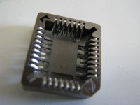
Dunno if those FTDI chips have enough pins to handle it though. I think I mentioned them briefly on one of the previous pages.I just took a look at my surface-mount PLCC sockets (picture below) and I see what everyone is talking about. The plastic gets in the way of the pins so a soldering iron is pretty much impossible. I think I saw a tutorial somewhere where someone cut out the bottom plastic stuff and was able to hand-solder them with an iron, so that might be an option for hand assembly...there isn't much space to work with in there, though!
How about putting a serial port/CPU chiplet on the SIMM . . .
. . . and hot-wiring it to the IIci's Modem Port?)
p.s. I don't have a IIci either . . . not yet anyway! [] ]'>
p.p.s. If that's the same size socket as the one for the DeclROM in the Duo MiniDock . . .
. . . there was a wire wrap version available! Thru-holes ROCK!!! :approve:
. . . and hot-wiring it to the IIci's Modem Port?
) p.s. I don't have a IIci either . . . not yet anyway! [
] ]'>p.p.s. If that's the same size socket as the one for the DeclROM in the Duo MiniDock . . .
. . . there was a wire wrap version available! Thru-holes ROCK!!! :approve:
I agree you can likely find a through-hole or wire-wrap version of that PLCC socket. That one you've pictured doesn't look so great for soldering!
I really like the idea of making the SIMM flashable over USB! Is there physical space for a mini-USB connector on the end of the SIMM?
You could use one of those FTDI chips, or any common AVR using the free V-USB software. If you program each of the four ROMs on the SIMM one at a time, then you'd need 8 bits of data, 16-ish bits of address (depending on your ROM size), 4 individual write enables, 4 individual output enables, and one combined chip select, so 33 total I/Os by my accounting. Probably too many for an AVR or the FTDI, but you could use one of those in combination with a few shift registers. Shift in the address+data, then manipulate the control lines to read/write a byte.
I really like the idea of making the SIMM flashable over USB! Is there physical space for a mini-USB connector on the end of the SIMM?
You could use one of those FTDI chips, or any common AVR using the free V-USB software. If you program each of the four ROMs on the SIMM one at a time, then you'd need 8 bits of data, 16-ish bits of address (depending on your ROM size), 4 individual write enables, 4 individual output enables, and one combined chip select, so 33 total I/Os by my accounting. Probably too many for an AVR or the FTDI, but you could use one of those in combination with a few shift registers. Shift in the address+data, then manipulate the control lines to read/write a byte.
:lol: I can just see it now! A 68030 based IIci with a freakin' USB Port installed on the backplane! )
I don't see why you couldn't design the SIMM to be higher a/o build an addition onto the inboard side . . .
. . . just make sure it stops off where the RAM SIMMs begin! }
) I don't see why you couldn't design the SIMM to be higher a/o build an addition onto the inboard side . . .
. . . just make sure it stops off where the RAM SIMMs begin! }
LOL...we could have some crazy board that hooks into a NuBus slot and the ROM SIMM slot at the same time!
Thanks for the tip on V-USB. I had never heard of it, and it looks VERY impressive! I like the idea of an AVR in charge of the whole thing.
I don't think any more chips/connectors period will fit on the SIMM unless they went on the opposite side. Would probably need 4 layers for that.
The only thing with through hole PLCC is I'm not sure that traces can fit between the pins if those are used. It might make the board more complicated to route.
I think I have a SIMM layout but it probably needs refinement. Anybody interested in taking a look at what I've got and critiquing it? I made it in FreePCB, so I could post the file or a screenshot or something...
Thanks for the tip on V-USB. I had never heard of it, and it looks VERY impressive! I like the idea of an AVR in charge of the whole thing.
I don't think any more chips/connectors period will fit on the SIMM unless they went on the opposite side. Would probably need 4 layers for that.
The only thing with through hole PLCC is I'm not sure that traces can fit between the pins if those are used. It might make the board more complicated to route.
I think I have a SIMM layout but it probably needs refinement. Anybody interested in taking a look at what I've got and critiquing it? I made it in FreePCB, so I could post the file or a screenshot or something...
I was laying out the different styles (SMT, through-hole) last night, and I am kind of mixed about which way to go. SMT would be easier to lay out but harder to assemble. I am thinking about doing a layout in Eagle CAD and having it open sourced like many Arduino projects. It would be cool if someone could check my work or join-in too. I can probably get an x-ray of a SIMM sometime soon to also use as a reference.
Almost done...


Haha, sounds like we're on the same page here! Are you talking about looking at an existing SIMM's layout? I think that would be helpful to see, even if just the top and bottom without having to x-ray it.
Here's what I have so far. I only have contacts on one side of the board but that should be easy to fix. I am thinking that the copper area for ground on the bottom layer is going to get sliced up pretty bad in the places where there are some traces bunched together on the bottom layer, so I should probably remove it from those spots? Also, I don't know if I put the capacitors close enough to the chips -- apparently they're supposed to be as close as possible? Maybe they could be on the other side of the board underneath the chips?
Any suggestions/critiques/whatever are totally welcome! I'm a newbie to board layout so I'm expecting to hear a lot of stuff that needs to be fixed. Or if trag or tt or whoever else has a better design I'm cool with that too
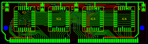
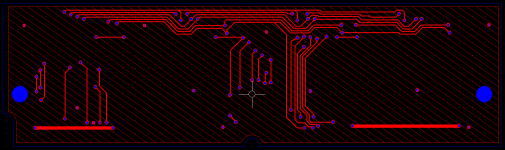
Any suggestions/critiques/whatever are totally welcome! I'm a newbie to board layout so I'm expecting to hear a lot of stuff that needs to be fixed. Or if trag or tt or whoever else has a better design I'm cool with that too
Here are my pics, sorry for the poor quality. I can take better ones later if needed.
The top ROM is from a IIfx and bottom ROM is from a IIsi:
Backs:

Fronts:

Wow, your CAD looks pretty close to complete! It looks like they use vias to get pads connected to the front and back when I look at the images more closely.
X-ray is not necessary, but I might have some extra machine time to use since the lab I work with charges a 1hr minimum. If the board designs are identical, then an image match is a good way to check to make sure everything is in the right place.
The top ROM is from a IIfx and bottom ROM is from a IIsi:
Backs:
Fronts:
Wow, your CAD looks pretty close to complete! It looks like they use vias to get pads connected to the front and back when I look at the images more closely.
X-ray is not necessary, but I might have some extra machine time to use since the lab I work with charges a 1hr minimum. If the board designs are identical, then an image match is a good way to check to make sure everything is in the right place.