

Thread
Another IIci ROM hack
Oh wow! Thanks for the scans! Those are very, very helpful! Glad to see Apple did a similar thing by using the bottom layer to connect the pins near the top of the PLCCs on the IIsi one, so I'm not totally crazy 
Ah that's true. I didn't realize it was convenient enough for you to do the X-rays. Cool!
Yeah, I noticed a similar thing with the vias on that LaserWriter ROM SIMM I got. Doesn't seem like it would be too bad to use a bunch of vias to stick the other side in place. Not sure how I'll connect some of those VCC pins together though...looks like Apple just left some of them not connected, so that would probably work.
Ah that's true. I didn't realize it was convenient enough for you to do the X-rays. Cool!
Yeah, I noticed a similar thing with the vias on that LaserWriter ROM SIMM I got. Doesn't seem like it would be too bad to use a bunch of vias to stick the other side in place. Not sure how I'll connect some of those VCC pins together though...looks like Apple just left some of them not connected, so that would probably work.
HEH! That'd be my job description!. . . so I'm not totally crazy
 )
) Don't bother putting pads on the backside of the board. As I understand it, the SIMM spec isn't as thick as the standard FRP blanks used by the fab houses. If there's no metal on the backside of the pad area, we can run them over a router bit as I described above, instead of filing away at them the way gamba had to do in order to get the gamba/trag SIMMs to fit.
You might want to move the plated thru holes to the backside far enough away from the front side pads to give a better margin of error for setting up a Router Table/Sliding Table combo.
What's the maximum possible size for an expanded area ROM SIMM for the IIci, SE/30 and IIsi? :?:
If anyone has all three machines, a cardboard mock-up that'll clear all obstacles when installed in those three machines would be a good starting point for an in-place programmable EEPROM setup.
I guess X-ray wouldn't help too much in this case since the IIsi ROM is also 512k, so it will be different for a 1Mb ROM according to Trag due to the different pin-out.
I think having pads on the front and back might be useful for redundancy/reliability in the socket. It would be a pain to diagnose if your machine doesn't boot one day just because of a marginal contact. It looks like dougg3 is designing it for fab at a board house. If the board fab says they can make the proper thickness, then why not just go for the whole package?
Overall it looks like the placement of components is good. Looks like the caps are moved over for clearance for sockets in case you want to use them? I can't comment on the actual connections. dougg3, did you have a schematic associated with the board or is it based on physical placement alone?
I think having pads on the front and back might be useful for redundancy/reliability in the socket. It would be a pain to diagnose if your machine doesn't boot one day just because of a marginal contact. It looks like dougg3 is designing it for fab at a board house. If the board fab says they can make the proper thickness, then why not just go for the whole package?
Overall it looks like the placement of components is good. Looks like the caps are moved over for clearance for sockets in case you want to use them? I can't comment on the actual connections. dougg3, did you have a schematic associated with the board or is it based on physical placement alone?
Haha, I think it fits me pretty well too!HEH! That'd be my job description!. . . so I'm not totally crazy
I agree, but bigmessowires pointed out a very reasonably-priced PCB place that *does* do the correct board thickness. So I may be able to get away with not having to worry about the thickness at all
Are you talking about the vias that are near the SIMM connectors? I should be able to do that pretty easily if we do end up having to use the router.
If all the lines are hooked up in the pinout that's shown in the wiki, there are 21 address lines that are actually used, for a total of 2^21 = 2*1024*1024 addresses, and each address actually points to four bytes, so that would be 4*2*1024*1024 bytes or 8 megabytes. Is my math right? The SIMM design I'm making hooks up all 19 of the standard PLCC32 address lines, which would allow for a maximum of 2 megabytes of ROM space if we used 4 megabit flash chips.
True, true! I didn't think about needing it to fit in the SE/30 and IIsi and whatever else there might be!
If the IIsi's ROM is 512 kilobytes in size, that means that it uses four 1 Megabit ROMs for a total of 4 megabits, or 512 kilobytes. Trag was saying that 1 megabit and bigger ROM chips use a different pinout from the 512 kilobit and smaller chips. Since the IIsi does use 1 megabit chips, the IIsi's SIMM should be spot on for the correct pinout
Except it probably won't have some of the higher address lines connected -- I'll check on that, but it shouldn't be too bad to add.As long as Seeed Studio works out, I definitely agree
Thanks! Yeah, that's why I moved the caps, to make room for the sockets. I'm definitely not against moving them elsewhere -- even to the back of the board if the need arises. I think they're supposed to be as close to the chip's pins as possible... No, I didn't use a schematic because FreePCB only does the board layout part of things.
 I'm probably crazy for not starting from a schematic...
I was actually asking about the physical size of an expanded PCB area. A higher and wider than normal ROM SIMM could enable addition of the extra gobble-de-gook necessary for doing a SIMM that's programmable while inside the box.
The overall shape of the PCB would have to be a bit funky to make it wider, but what about this hack isn't?)
The overall shape of the PCB would have to be a bit funky to make it wider, but what about this hack isn't?
) Oh yeah, thanks for clarifying, I am getting bits and bytes confused. I'll x-ray the board in any case if I can. If it doesn't help, it will at least be a cool image for the collection. I might also x-ray a IIcx DayStar socket board as well, but that's another topic.
Yeah, it is a sweet deal. With prices that low, I would even spring for a sporty red color. }
I would do it that way if there is no schematic avail, but I am crazy.I'm probably crazy for not starting from a schematic...
I'd forgotten about all the little notches you'll need on the SIMM, which you can see in tt's photo. You'll need to include those in the board outline, unless you plan to use a router tool to cut them yourself afterwards. One problem is that I'm pretty sure Seeed only does rectangular boards for the price they offer-- that's part of why it's so cheap. I think Batch PCB and Dorkbot PDX will do arbitrary board outlines, but I'm not sure if they offer the 1.2mm thickness you need. You may have to hunt a little to find a place that will do arbitrary outlines *and* 1.2mm thickness for a reasonable cost for a hobbyist, but I'm sure it's doable.
Your layout looks pretty good to me. I wouldn't sweat the capacitor placement too much-- closer to the power pins is better, but it'll probably still work fine even if they're further out.
If you do get the 1.2mm thick board, then I'd suggest putting contact pads on both sides, like you planned.
I don't think you should need a 4-layer board. If you have trouble fitting all the traces, try the method of routing everything on the top side horizontally and bottom side vertically, with no diagonal traces.
Your layout looks pretty good to me. I wouldn't sweat the capacitor placement too much-- closer to the power pins is better, but it'll probably still work fine even if they're further out.
If you do get the 1.2mm thick board, then I'd suggest putting contact pads on both sides, like you planned.
I don't think you should need a 4-layer board. If you have trouble fitting all the traces, try the method of routing everything on the top side horizontally and bottom side vertically, with no diagonal traces.
Their description implies that they accommodate slots:
In other words, larger slots are okay, but no really long slots are allowed. The little notches needed by a SIMM should be fine.
Use really thick traces for the capacitors. One thing you can do is put something like a 39 mil via on end of the Vdd and Vcc pins and put the capacitors on the back of the board, right next to the vias.
I agree. Two layers should work fine. My Mac IIfx SIMMs are two layers and they work.
If you look at this image, between the first and second chips from the left, you'll see a bypass cap connected with relatively long thick traces. Also, note the copper fill around the edges of the board.

In the following picture, you can see the bypass cap for the other memory chip near the center of the board. Again, note the fill around the edges and sometimes near the middle of the board. I filled Vcc on the front of the SIMMs and Vdd on the back.

Same thing, but different model, and slightly cleaner layout, because there was more repetition:


Yeah, my board outline is in the screenshots, it's just dark blue so it's hard to see. I also noticed that on Seeed Studio's forums someone asked about making a circular board or a board with rounded edges and those both seemed fine. So I think they will be able to do it I'll definitely put contacts on both sides now.
Good idea about putting the capacitors on the back of the board with the thick traces between the ground and VCC pins. I'll go for it.
I noticed on tt's picture of the IIsi ROM SIMM, the VCC trace out of the SIMM contacts is really thin. I was planning on making the VCC traces a lot thicker as you can see from my design. Probably doesn't matter but I'd rather be safe than sorry!
Looks indeed like 2 layer will be fine. I was just nervous because my original design was more complicated than it needed to be. I like the idea of ground fills on one side and VCC fills on the other. Doesn't that basically make the board a big capacitor, too? Anyway, I'll see what I can do!
Nice pics, trag! Those are awesome 64 pin IIfx SIMMs. Thanks for showing your designs!
My coworker also suggested moving the vias that are really close to the PLCC pads (like on the ground pins on my screenshot) away a bit so if we do the reflow stuff, the solder won't flow into the via. He also said he thinks he could probably hand solder one of those surface mount PLCC sockets but it would be tough. We'll see...
I'll definitely put contacts on both sides now.Good idea about putting the capacitors on the back of the board with the thick traces between the ground and VCC pins. I'll go for it.
I noticed on tt's picture of the IIsi ROM SIMM, the VCC trace out of the SIMM contacts is really thin. I was planning on making the VCC traces a lot thicker as you can see from my design. Probably doesn't matter but I'd rather be safe than sorry!
Looks indeed like 2 layer will be fine. I was just nervous because my original design was more complicated than it needed to be. I like the idea of ground fills on one side and VCC fills on the other. Doesn't that basically make the board a big capacitor, too? Anyway, I'll see what I can do!
Nice pics, trag! Those are awesome 64 pin IIfx SIMMs.
Thanks for showing your designs!My coworker also suggested moving the vias that are really close to the PLCC pads (like on the ground pins on my screenshot) away a bit so if we do the reflow stuff, the solder won't flow into the via. He also said he thinks he could probably hand solder one of those surface mount PLCC sockets but it would be tough. We'll see...
It can definitely be hand-soldered. I've hand-soldered SMT PLCC chips, as well as QFP chips with even smaller pin spacing (down to 0.5mm spacing). I used the "drag solder" technique with a standard soldering iron. Google for video demos if you're not familiar with the technique. A toaster over reflow would probably work too, but I've never done that myself.
Oh I know it can be done when the chips are out in the open (I've done it too with a 0.5 mm LQFP), but I mean he says he can get the pins soldered despite the plastic socket material being in the way, like from that picture I posted the other day. I don't think the drag method would work since those little plastic doodads are there between some of the pins. I figured the plastic being in the way would be a showstopper, but he thinks he can squeeze in there and still solder it. Either way it will be a pain for assembly, though.
The oven reflow works pretty well, especially if you have a solder paste stencil so you can just squeegee solder paste on, stick on the parts, and bake it.
The oven reflow works pretty well, especially if you have a solder paste stencil so you can just squeegee solder paste on, stick on the parts, and bake it.
Here's the x-ray of a IIsi ROM:
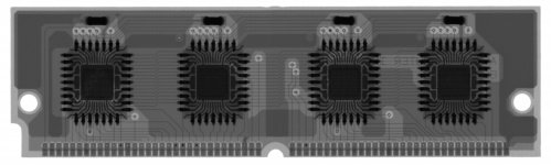
Haha, that is awesome! Not only is it very useful, but it is really cool to see! Thanks for x-raying it!
I really like how you can see inside the PLCC chips.
I really like how you can see inside the PLCC chips.
It's probably too late to help, but here is the front layer of my SE/30 ROM layout. It may be incomplete, such as missing connections or details remaining to be fixed. Apparently the last time I worked on this was September of 2006.

And the back layer:

The file with the design in it is in this folder:
http://www.prismnet.com/~trag/Classic%20Mac
I used Osmond PCB for the design, which is excellent Mac based PCB layout software:
http://www.osmondpcb.com/index.html
When I started using it, it was in Beta and free. After it went commercial, I bought a copy for $200 and consider it well worth it. Apparently it is $79 now.
You can download Osmond and use it to open my design. Without purchasing license you won't be able to print it, I think. If it's under 700 pins then it will be printable/exportable.
And the back layer:
The file with the design in it is in this folder:
http://www.prismnet.com/~trag/Classic%20Mac
I used Osmond PCB for the design, which is excellent Mac based PCB layout software:
http://www.osmondpcb.com/index.html
When I started using it, it was in Beta and free. After it went commercial, I bought a copy for $200 and consider it well worth it. Apparently it is $79 now.
You can download Osmond and use it to open my design. Without purchasing license you won't be able to print it, I think. If it's under 700 pins then it will be printable/exportable.
Since we're also on the subject of IIfx SIMMS all of a sudden . . . [ ] ]'>
] ]'>
I always wanted to look into hijacking the parity lines by cutting them at the memory controller and patching them to any available/unused bank/row select pins to increase the capacity of a custom SIMM design to make use of the extra signals which would suddenly become available at the SIMM Slot level and as quiet as a church mouse running through the parity traces.
IIrc the fx has something like a 1G memory space . . .
. . . whatcha think trag? }
] ]'>I always wanted to look into hijacking the parity lines by cutting them at the memory controller and patching them to any available/unused bank/row select pins to increase the capacity of a custom SIMM design to make use of the extra signals which would suddenly become available at the SIMM Slot level and as quiet as a church mouse running through the parity traces.
IIrc the fx has something like a 1G memory space . . .
. . . whatcha think trag? }
No idea on jt's question...I'll leave that for trag and the other hardware experts
I have been looking at the Apple SIMMs and the X-ray image. I was completely wrong about VCC's traces being thin. They are nice and thick -- and it appears the IIsi ROM SIMM has more than 2 layers. If I'm not mistaken, there is a VCC plane in the middle of the board, and maybe a ground plane in the middle of the board too. Can anyone confirm that? Here are my reasons:
So it may be better to stick with something closer to my original design and/or trag's design that he just shared.
I have been looking at the Apple SIMMs and the X-ray image. I was completely wrong about VCC's traces being thin. They are nice and thick -- and it appears the IIsi ROM SIMM has more than 2 layers. If I'm not mistaken, there is a VCC plane in the middle of the board, and maybe a ground plane in the middle of the board too. Can anyone confirm that? Here are my reasons:
- I don't see any connections between the VCC pins on each chip (3rd from the right on the top when looking at the image of the top) to any other chips, but each one of them has a via (3 of them are hidden under the chips) that seemingly goes to nothing -- it's not connected to anything on the bottom layer. That kind of hints that there's another plane running underneath the board.
- All of the VCC pads on the SIMM connector don't go to anything on the top or bottom layer.
- The ground pins on the first and third chips from the left have vias that also seemingly go nowhere. So they must be going to some kind of a ground plane underneath...
So it may be better to stick with something closer to my original design and/or trag's design that he just shared.
By George, I think you've got it! :approve:
Take a look at the bottom right corner of the X-Ray. It clearly shows three different planes by the beginnings and ends of their shading overlaps.
Take a look at the bottom right corner of the X-Ray. It clearly shows three different planes by the beginnings and ends of their shading overlaps.
Ah, that's right! You can see a similar thing on the left side of the board too. I still can't get over how cool that X-ray image is 
Yes, I was wondering about the number of layers last night while I was playing around with trace routings, some things were not quite making sense if the board was just 2 layers.
Thanks Trag for posting your design! Maybe we should all collectively vet one design and generate gerber files after its confirmed to appear correct.
Is there a schematic for the ROM somewhere?
Thanks Trag for posting your design! Maybe we should all collectively vet one design and generate gerber files after its confirmed to appear correct.
Is there a schematic for the ROM somewhere?
No schematic for my design. I usually do what amounts to a netlist on the fly. After I've created the parts in Osmond, I connect all the pads that need connecting, which results in what's called a Rat's Nest.
You can't see it on the images I captured, but the edge connector for the ROM is a Part, and the PLCC32 chips are Parts, and there's a view mode in Osmond which will show the pin numbers (and names, if you've entered them). That view mode is pretty handy for creating the Rat's Nest.
Once the Rat's Nest is created, it's just a matter of dragging the traces all over the place, until you meet the design rules. Of course, one ends up pushing some of the traces through vias, and that is a little more complicated than dragging a trace, but Osmond remembers what's supposed to make electrical connections, so it's pretty easy to cut a trace on one side of the board and see where to pick it up on the other side.
You can't see it on the images I captured, but the edge connector for the ROM is a Part, and the PLCC32 chips are Parts, and there's a view mode in Osmond which will show the pin numbers (and names, if you've entered them). That view mode is pretty handy for creating the Rat's Nest.
Once the Rat's Nest is created, it's just a matter of dragging the traces all over the place, until you meet the design rules.
Of course, one ends up pushing some of the traces through vias, and that is a little more complicated than dragging a trace, but Osmond remembers what's supposed to make electrical connections, so it's pretty easy to cut a trace on one side of the board and see where to pick it up on the other side.
Better photos:
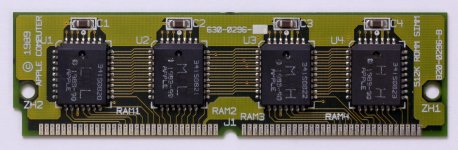
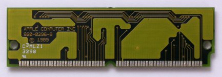
Very nice close-up pics! I actually designed my board pretty much the same way trag said. I probably would have started from a schematic except the app I'm using is only for board layout. But for this particular board, the schematic would be kind of pointless anyway. It's basically "hook all the corresponding lines on each chip together except for the data lines", and then find a place somewhere to connect each SIMM pad to its corresponding net. I found the 64-pin SIMM part in EAGLE, and copied it into FreePCB manually by looking at the coordinates of all the vertices.
Here's what I have now after cleaning up the ground copper fill on the bottom layer, adding a VCC copper fill to the top layer, moving the capacitors to the bottom close to the PLCC chips, and a few other minor fixes:
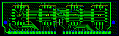
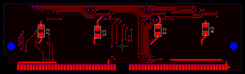
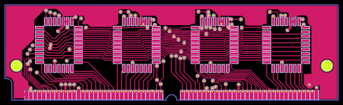
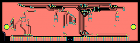
Not sure if I'm happy with the placement of some of the vias near the PLCC pads. It's hard to find room! I was designing these vias with the minimum acceptable size for BatchPCB so that's why they might be kind of big. I can't fit them when they're that big. Maybe with Seeed Studio I can go smaller.
Here's what I have now after cleaning up the ground copper fill on the bottom layer, adding a VCC copper fill to the top layer, moving the capacitors to the bottom close to the PLCC chips, and a few other minor fixes:
Not sure if I'm happy with the placement of some of the vias near the PLCC pads. It's hard to find room! I was designing these vias with the minimum acceptable size for BatchPCB so that's why they might be kind of big. I can't fit them when they're that big. Maybe with Seeed Studio I can go smaller.
Is there anything a liberal arts major can help with? If you get any boards printed, I could make a nifty logo to be screened onto it. 
Absolutely olePigeon! Every project needs a liberal arts major to do all the awesome artsy stuff! If you want to put something together I would be thrilled to stick it on the board if I can figure out how. That would be cool! As long as it isn't something like Apple's logo that could get me in trouble
I just realized I'm an idiot and I should have used Eagle to make this board. For some reason I thought my board was wider than 4 inches (it's not) so Eagle's free version wouldn't work (it will). Maybe I thought I'd need 4 layers too. Whatever...I'm going to stick with FreePCB because I'm pretty familiar with it now but Eagle really would have been a smarter choice in hindsight.
I'm starting to think I'd like to get a few of these made so I can at least see if it's going to work. This is my first ever PCB so I'm kind of excited to try it. I'm sure you guys know the feeling.
It looks like it's going to cost:
$9.90 for the base price of 10 boards (don't want to buy more than 10 initially in case I made a mistake)
+ $15 because it's bigger than a 5cm by 5cm square (it fits in a 10cm by 5cm rectangle)
+ $10 for a custom color (we have to do something other than boring green! They have blue, white, red, and yellow)
for a total of:
$34.90
If my calculations are correct (I was a math minor, so they better be!) ;-)
That's an amazing price for PCBs. I'll go ahead and eat the cost of that, and we'll see where things go! I'm going to wait a bit before doing an order though so we can get on the same page, I like tt's idea of working together to get a good design to go with. Where should we go from here?
If you want to put something together I would be thrilled to stick it on the board if I can figure out how. That would be cool! As long as it isn't something like Apple's logo that could get me in trouble I just realized I'm an idiot and I should have used Eagle to make this board. For some reason I thought my board was wider than 4 inches (it's not) so Eagle's free version wouldn't work (it will). Maybe I thought I'd need 4 layers too. Whatever...I'm going to stick with FreePCB because I'm pretty familiar with it now but Eagle really would have been a smarter choice in hindsight.
I'm starting to think I'd like to get a few of these made so I can at least see if it's going to work. This is my first ever PCB so I'm kind of excited to try it. I'm sure you guys know the feeling.
It looks like it's going to cost:
$9.90 for the base price of 10 boards (don't want to buy more than 10 initially in case I made a mistake)
+ $15 because it's bigger than a 5cm by 5cm square (it fits in a 10cm by 5cm rectangle)
+ $10 for a custom color (we have to do something other than boring green! They have blue, white, red, and yellow)
for a total of:
$34.90
If my calculations are correct (I was a math minor, so they better be!) ;-)
That's an amazing price for PCBs. I'll go ahead and eat the cost of that, and we'll see where things go! I'm going to wait a bit before doing an order though so we can get on the same page, I like tt's idea of working together to get a good design to go with. Where should we go from here?
If you're not putting any self-programmable goodies on this version, could you switch to the through-hole style of the PLCC socket? That might help address your worries about soldering it. Or were you planning to solder the ROMs directly without using a socket... in which case they can never be reprogrammed, right?
True, true. I'll look at the through hole versions for the basic design. Who knows, it might even simplify the routing!
HEY, OleWingedRat! Watch it! I resemble that remark! [Is there anything a liberal arts major can help with? If you get any boards printed, I could make a nifty logo to be screened onto it.
] ]'>Being a liberal arts major has some pretty cool advantages, especially a Jesuit Liberal Arts Degree. Those ole' coots turn kids who've they've taught to THINK loose into the world.
Like Charlie Rose! :approve:
A good general education helps in learning all kinds of interesting crap for the rest of your life!
)
The more I play around with the through hole PLCC sockets the more I'm starting to believe it's a nightmare to route, especially with only 2 layers. I'm starting to see why everybody started going toward SMT...
It's just that with so many pins per row, it's really tough to find enough places to squeeze traces between the pins to get the signals across the board. The SIMM will definitely have to be taller; not sure if that's a problem or not in some of the Macs. It's also nearly impossible to put the capacitors directly on the other side of the board underneath the sockets.
I think if we go the through hole route I'm going to have to let someone more experienced with PCB layout take the reins!
It's just that with so many pins per row, it's really tough to find enough places to squeeze traces between the pins to get the signals across the board. The SIMM will definitely have to be taller; not sure if that's a problem or not in some of the Macs. It's also nearly impossible to put the capacitors directly on the other side of the board underneath the sockets.
I think if we go the through hole route I'm going to have to let someone more experienced with PCB layout take the reins!
Fuggedaboudit! :lol:
In the bad 'ole thru hole days, it was not uncommon to see discrete wire legged, color coded noise caps stretched across the diagonal of a fairly large DIP IC.
Just put an extra thru-hole on the GND and VCC "pads" . . .
. . . and use that same ancient trick running them underneath your socket! }
In the bad 'ole thru hole days, it was not uncommon to see discrete wire legged, color coded noise caps stretched across the diagonal of a fairly large DIP IC.
Just put an extra thru-hole on the GND and VCC "pads" . . .
. . . and use that same ancient trick running them underneath your socket! }
Are you talking like axial electrolytic capacitors, or something else? What kind of capacitor could I use? Either way, I like it! I didn't even consider just skipping surface mount capacitors. With the through hole sockets, it may be easier just to use through hole capacitors as well. Pretty cool I think this may work out OK actually.
I was getting frustrated with the through hole PLCC sockets, but I'm starting to get more comfortable with them -- looks like I can fit 2 traces between pins. Also bigmessowires' hint about going horizontal in one layer and vertical in the other layer is turning out to be VERY useful. I have had to make my board taller to make room for more stuff, but it's starting to feel possible!
I think this may work out OK actually.I was getting frustrated with the through hole PLCC sockets, but I'm starting to get more comfortable with them -- looks like I can fit 2 traces between pins. Also bigmessowires' hint about going horizontal in one layer and vertical in the other layer is turning out to be VERY useful.
I have had to make my board taller to make room for more stuff, but it's starting to feel possible!