

Thread
Designing a portable RAM card
Hmm. Purple. Sonnet style. Nice that actually doesn't sound bad.
went ahead and asked for a quote for 5 pcs prototyping run, just to gauge an idea what each PCB is going to cost roughly. Then i get a bill of materials together, price of RAM from trag, and then assembly/test labor which at that point I can get a per piece price.
I make a poll to see whos interested in buying, so then I can justify the cost of running the boards.
of course, the PCBs might be cheaper if I order a larger number of them, or if I actually panelized the layout, but eh.. thats alot of work.
I make a poll to see whos interested in buying, so then I can justify the cost of running the boards.
of course, the PCBs might be cheaper if I order a larger number of them, or if I actually panelized the layout, but eh.. thats alot of work.
Count me in! I need this and a new ribbon cable (plus a hard drive) to get my Portable 100%.
Money is something I don't have in abundance at the moment, however, so it'll probably be awhile.
But I'm definitely interested!
c
Money is something I don't have in abundance at the moment, however, so it'll probably be awhile.
But I'm definitely interested!
c
Yup, hopefully itll be cheap enough to hold interest. Otherwise i designed it all for nothing haha.
my next goal is to design an asyncronouse memory-mapped I/O PDS card.
So i can read/write specific addresses to read/write the card.
I dont really want to mess with DeclROMs, slot manager, slots, all that jaz that most cards do. Id rather just have simple peripheral cards that are directly addressed via drivers.
The next step toward a ARM co-processor/raspberry pi PDS card.
my next goal is to design an asyncronouse memory-mapped I/O PDS card.
So i can read/write specific addresses to read/write the card.
I dont really want to mess with DeclROMs, slot manager, slots, all that jaz that most cards do. Id rather just have simple peripheral cards that are directly addressed via drivers.
The next step toward a ARM co-processor/raspberry pi PDS card.
awesome man… yeah purple is should be pretty cool...
count me in for 2.
count me in for 2.
I vote for Red
Well, I got quoted for 5 boards, at $62.50. This is basic green. different colors cost more.
$37 for the boards, and another 25 for shipping from china. sheesh. all the board houses are in china these days. Even imagineering is, which is who I used for our production boards for Major Display LLC.
$37 for the boards, and another 25 for shipping from china. sheesh. all the board houses are in china these days. Even imagineering is, which is who I used for our production boards for Major Display LLC.
Yeah, dealing with China can be expensive in shipping costs and shipping time (up to 6 weeks or more to go through customs? Sheesh!) But they are cheap otherwise.
TechKnight, copyright your design (send 2-self addressed mailed planes to yourself and open one up to see it and keep the other sealed until a "judge needs to see it," and keep both together) and then get an application to send a copy to the Copyright Office at the Library of Congress. Last time I had something copyrighted by the LoC was in the 1990s and cost $14, I don't know what it is now. I understand that you are doing this for the community and all, but its best to protect your ideas. It's nice to have that "by © year" with your name on it on what you put out.
TechKnight, copyright your design (send 2-self addressed mailed planes to yourself and open one up to see it and keep the other sealed until a "judge needs to see it," and keep both together) and then get an application to send a copy to the Copyright Office at the Library of Congress. Last time I had something copyrighted by the LoC was in the 1990s and cost $14, I don't know what it is now. I understand that you are doing this for the community and all, but its best to protect your ideas. It's nice to have that "by © year" with your name on it on what you put out.
I can't even wait!!!!!!!!!!!!!!! You are the bomb Techknight!!!!!!!!!!! I may buy 8 if I can afford them...  and if you produce enough..
and if you produce enough..
Could I entice you to put a Jolly Roger around those diagnostic LEDs? 

The Jolly Roger image would look cool on it....
For the proto-type(s), whatever color will be easiest on your eyes when you are soldering and provide the best background, with respect to visibility of the soldering.
As long as I dont find any more errors ill run the boards.
Get a BOM together and figure out the cost per board from there.
Hey trag can you message me the chip prices so I can factor that in.
Get a BOM together and figure out the cost per board from there.
Hey trag can you message me the chip prices so I can factor that in.
PCB Express here in the US and Shennan Ckts in China.. High quality.. shennan takes gerber files and will convert and PCB express requires you draw with their software.. Which is free.. A friend uses these guys
I used to use ExpressPCB but I quit because its proprietary. Much easier than eagle though, but i rather use something that renders industry standard files.
plus expressPCB is very expensive.
I was using iTead with prototype runs, because it was cheap. but one of the guys split off and started his own thing, and i got a quote from him.
plus expressPCB is very expensive.
I was using iTead with prototype runs, because it was cheap. but one of the guys split off and started his own thing, and i got a quote from him.
BTW, the diagnostic LEDs will likely be programatically hooked up to each chip select. So youll see them flash during the RAM test, or during read/writing in that RAM space.
flashing lights makes it look more important!

Whoops. Almost royally screwed up. Got to make a design change.
These are 2MB chips. the on-board RAM is only 1 MB in size, and the decoding to external address space starts at 2MB. Problem is, the New RAM is 20 bits in size, while the original is a total of 19 bits in size. So, if I leave A19 of the toshiba RAM hooked into A20 of the original addressing space, that would kill off the first 1MB on my toshiba chip, basically wasting half the chip, as A20 would be high when moving into external addressing. Since A20 is routed to the toshiba chips, well yea....
So, I am going to have to break off A20 from the RAM. Leaving the RAM only accessing in 1MB chunks. Then, move A20 to the CPLD and do some 1-2 decoding to use the full address space.
Wow... good thing I caught that. Doing the CPLD work is what made me think of this.
This is precisely the reason that when using memory modules in computers, they all have to be "equal"
Elfin: Even if I did copyright it, whos got the money to hire a bunch of lawyers and court proceedings to fight an infringement? I dont, so who cares? Plus this is strictly a niche market with a small yield so it doesnt really matter.
These are 2MB chips. the on-board RAM is only 1 MB in size, and the decoding to external address space starts at 2MB. Problem is, the New RAM is 20 bits in size, while the original is a total of 19 bits in size. So, if I leave A19 of the toshiba RAM hooked into A20 of the original addressing space, that would kill off the first 1MB on my toshiba chip, basically wasting half the chip, as A20 would be high when moving into external addressing. Since A20 is routed to the toshiba chips, well yea....
So, I am going to have to break off A20 from the RAM. Leaving the RAM only accessing in 1MB chunks. Then, move A20 to the CPLD and do some 1-2 decoding to use the full address space.
Wow... good thing I caught that. Doing the CPLD work is what made me think of this.
This is precisely the reason that when using memory modules in computers, they all have to be "equal"
Elfin: Even if I did copyright it, whos got the money to hire a bunch of lawyers and court proceedings to fight an infringement? I dont, so who cares? Plus this is strictly a niche market with a small yield so it doesnt really matter.
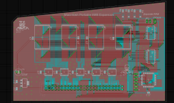
CPLD code is done, now its just a matter of waiting for the PCBs, assembly, JTAG programming, and test...
Ordered the PCBs, which pretty much depleted my budget.
Soon as I get some extra cash, I can order up the parts from digikey to finish the boards.
Soon as I get some extra cash, I can order up the parts from digikey to finish the boards.
techknight, just in case nobody said it recently, you are awesome!
Huzzah! Too awesome.
I can say, with true and absolute certainty, that this hasn't been accepted as evidence in patent court for at least 40 years, if not longer.
I think Elfen missed a step. It has to be notarized because it needs a witness to the contents.
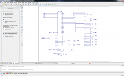
Here is my CPLD code in a nutshell:
Chip Select/Bank Select Signals.
A20, A21, A22, A23 Address line decode. The chip is hooked up between A0 and A18, or A1 to A19 if you look at the portable bus.
Base RAM:
0000 = No chip selected, all lines off = 0
Extended RAM:
0001 - Chip 1 Select ON, Lower Bank ON = 1
0010 = Chip 1 Select ON, Upper Bank ON = 2
0011 = Chip 2 Select ON, Lower Bank ON = 3
0100 = Chip 2 Select ON, Upper Bank ON = 4
0101 = Chip 3 Select ON, Lower Bank ON = 5
0110 = Chip 3 Select ON, Upper Bank ON = 6
0111 = Chip 4 Select ON, Lower Bank ON = 7
1000 = Chip 4 Select ON, Upper Bank ON = 8
When I say Upper/Lower bank, I mean just toggling A20 high or low. Since the macintosh portable has base RAM at 512K-Word, or 1MB, I decided to break the expansion down into 1 meg chunks as well. Since the toshiba chips are 1M-Word, or 2Mbytes, just deciding where A20 is determines if I am working with the first 512kword, or the second 512kword.
Chip Select/Bank Select Signals.
A20, A21, A22, A23 Address line decode. The chip is hooked up between A0 and A18, or A1 to A19 if you look at the portable bus.
Base RAM:
0000 = No chip selected, all lines off = 0
Extended RAM:
0001 - Chip 1 Select ON, Lower Bank ON = 1
0010 = Chip 1 Select ON, Upper Bank ON = 2
0011 = Chip 2 Select ON, Lower Bank ON = 3
0100 = Chip 2 Select ON, Upper Bank ON = 4
0101 = Chip 3 Select ON, Lower Bank ON = 5
0110 = Chip 3 Select ON, Upper Bank ON = 6
0111 = Chip 4 Select ON, Lower Bank ON = 7
1000 = Chip 4 Select ON, Upper Bank ON = 8
When I say Upper/Lower bank, I mean just toggling A20 high or low. Since the macintosh portable has base RAM at 512K-Word, or 1MB, I decided to break the expansion down into 1 meg chunks as well. Since the toshiba chips are 1M-Word, or 2Mbytes, just deciding where A20 is determines if I am working with the first 512kword, or the second 512kword.
I just want to say this is very cool. I was going to offer some suggestions, but everything already looks great to me.